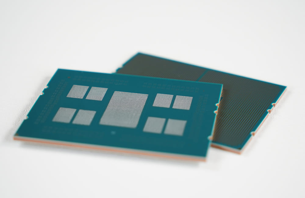
Samsung Electro-Mechanics is collaborating with Qualcomm to develop a 2.1D advanced packaging solution tailored for AI semiconductor chips. The companies have been working on this heterogeneous integration platform for over a year, focusing on research and validation processes.
The new packaging technology utilizes an embedded organic bridge. This design approach draws inspiration from Intel's Embedded Multi-die Interconnect Bridge (EMIB) but replaces the silicon bridge with more cost-effective organic materials. This strategy aims to reduce manufacturing expenses while avoiding potential patent conflicts with Intel.
The organic bridge functions as a small substrate featuring five to seven layers of micro-circuits created through the redistribution layer (RDL) process. Technical targets for this component include a line width and spacing of 1.5 to 2 micrometers, via sizes of 4 to 5 micrometers, and a pattern density of 500 to 1000 per square millimeter.
Compared to traditional flip-chip ball grid array (FC-BGA) stacked circuits, the organic bridge architecture enables finer wiring. This improvement facilitates higher input/output bandwidth, which is critical for the performance of advanced AI semiconductor applications.