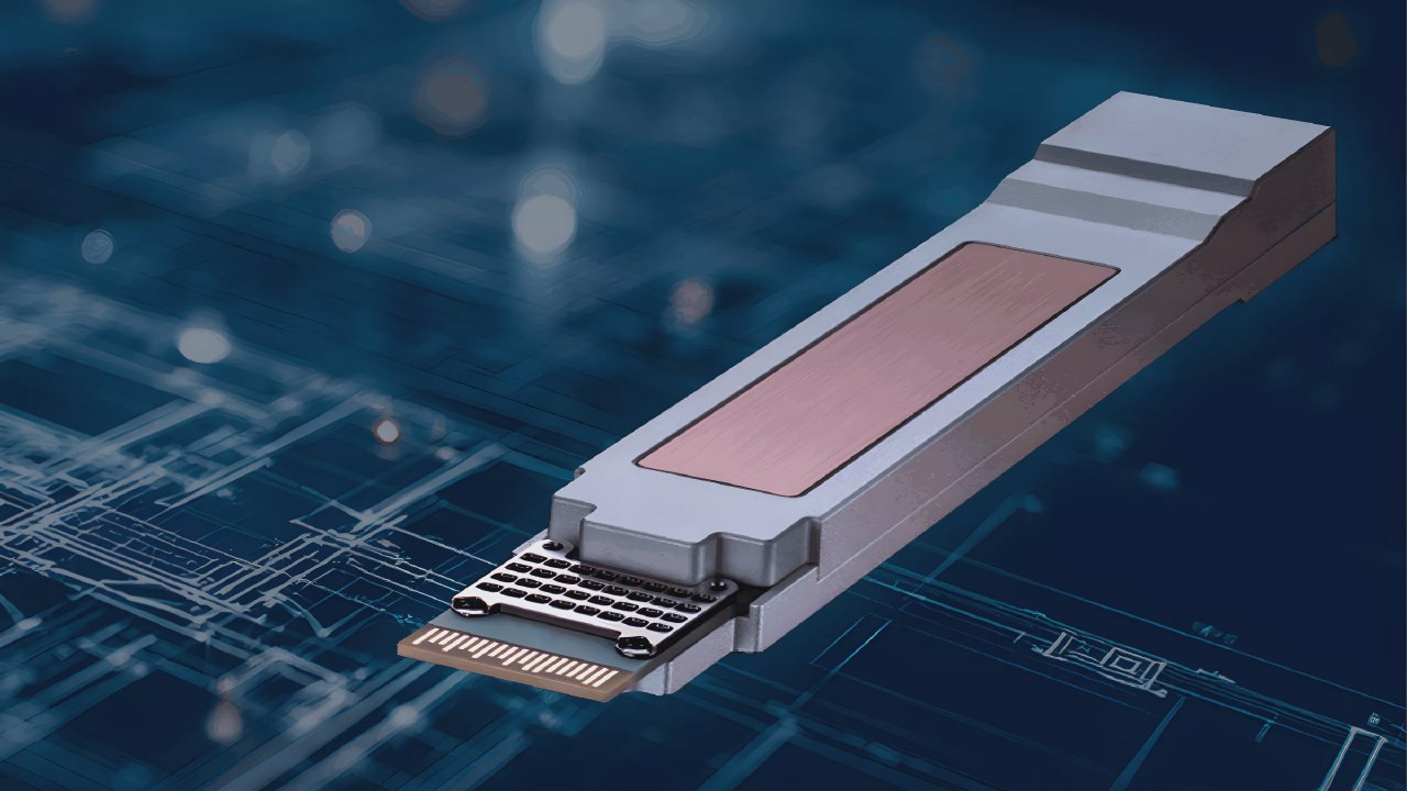
IBM is developing a 0.7 nm manufacturing process, known as Nanostack or CFET, to succeed current 2 nm technology. This architecture utilizes a 3D design where complementary transistor pairs are stacked vertically rather than placed side-by-side. The company estimates this approach could allow for 100 billion transistors on a 150 mm2 chip, offering a 50% performance increase or a 70% reduction in power consumption compared to 2 nm chips.
To address the design complexities of this new architecture, IBM is partnering with Siemens. Siemens, which entered the EDA market through its $4.5 billion acquisition of Mentor Graphics in 2017, will assist in developing the necessary design tools. The collaboration aims to help engineers manage challenges like parasitic capacitance and thermal interactions inherent in stacked component designs.
IBM plans to release a pilot Process Design Kit (PDK) in the first quarter of 2027. This kit will include standard logic cell libraries and SRAM arrays to allow developers to experiment with layouts and estimate performance before the technology matures. The company expects the practical implementation of the 0.7 nm process to occur no later than 2031.