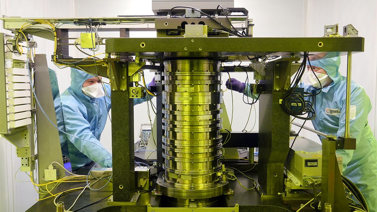
The Zelenograd-based ZNTC has completed a prototype of a domestic photolithography system designed for a 130nm process. The project received funding of approximately $70 million from the Russian Ministry of Industry and Trade. The system was developed in collaboration with the Belarus-based company Planar, which handled mechanical assemblies, and Lassard, which provided the lasers.
The estimated cost for a single ZNTC stepper is $6.7 million, with the laser light source adding another $600,000, totaling $7.3 million per unit. The machine is designed for 200-mm wafers. For comparison, the ASML PAS 5500/150 stepper, released in 2001, would cost roughly $5.8 million in current terms when adjusted for inflation.
The prototype was delivered five months behind schedule and is currently undergoing internal engineering and acceptance testing. The development of the lithographic process, including resist and mask qualification, remains ongoing. Experts suggest that the system is still years away from commercial use, with production deployment unlikely to occur before 2029.
While the 130nm node was adopted by major manufacturers like Intel and AMD in the early 2000s, this project represents a significant step for domestic engineering capabilities. ZNTC is now tasked with finalizing the design and ensuring the reliability and throughput of the equipment before it can be qualified for volume semiconductor manufacturing.