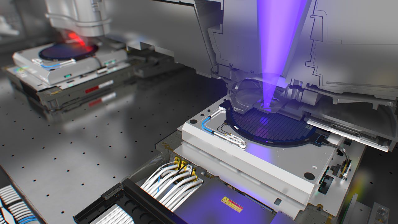
Intel has reached a milestone by processing over one million wafers using High-NA EUV lithography tools. This figure encompasses all wafers handled during tool installation, certification, research and development, and production phases. The company currently operates two ASML Twinscan EXE:5000 scanners and at least one EXE:5200B unit, which are utilized for the 18A process technology and the production of Panther Lake processors.
The company's cumulative output exceeds that of the rest of the industry combined. According to ASML, all High-NA EUV scanners shipped globally by April had processed over 500,000 wafers with an availability rate exceeding 80%. Intel's progress is significant, as the company increased its utilization from 30,000 wafers in February 2025 to over one million by September 2026.
To address the limitations of current High-NA EUV technology, which requires a process known as stitching due to the smaller exposure field of 6x6-inch masks, Intel is advocating for the adoption of larger 6x12-inch photomasks. Stitching currently reduces throughput on the EXE:5200B scanner from 175 to 125 wafers per hour and introduces complexities in chip design and alignment.
Transitioning to 6x12-inch masks would necessitate extensive modifications across the semiconductor supply chain, including mask blanks, inspection systems, and handling equipment. While ASML's current roadmap through 2033 focuses on 6x6-inch reticles, Intel is positioning itself as a leader in defining new standards for projection lithography to improve production efficiency and reduce costs.