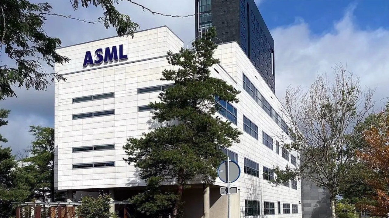
ASML continues to rely on laser-produced plasma (LPP) technology for its EUV lithography systems. Current setups utilize CO2 laser pulses fired at molten tin droplets, which are approximately 30 microns in diameter. The process generates 13.5-nm EUV radiation, which is then directed through a vacuum-sealed optical path using reflective mirrors.
The company has successfully increased the power of its LPP light sources from 250W to 500W. Future development plans include reaching a power output of 1000W and increasing the frequency of tin droplet generation to 100,000 droplets per second.
While free-electron laser (FEL) technology is being explored as an alternative that could eliminate the need for tin droplets and offer higher power, ASML remains focused on LPP. FEL systems require complex particle accelerators and advanced beam-distribution infrastructure, posing significant challenges in terms of cost and operational reliability.
Industry experts suggest that FEL technology is unlikely to compete with established LPP methods in semiconductor manufacturing for at least a decade. The development of such systems is expected to require investments reaching billions of dollars, creating substantial financial risks for companies currently pursuing this path.