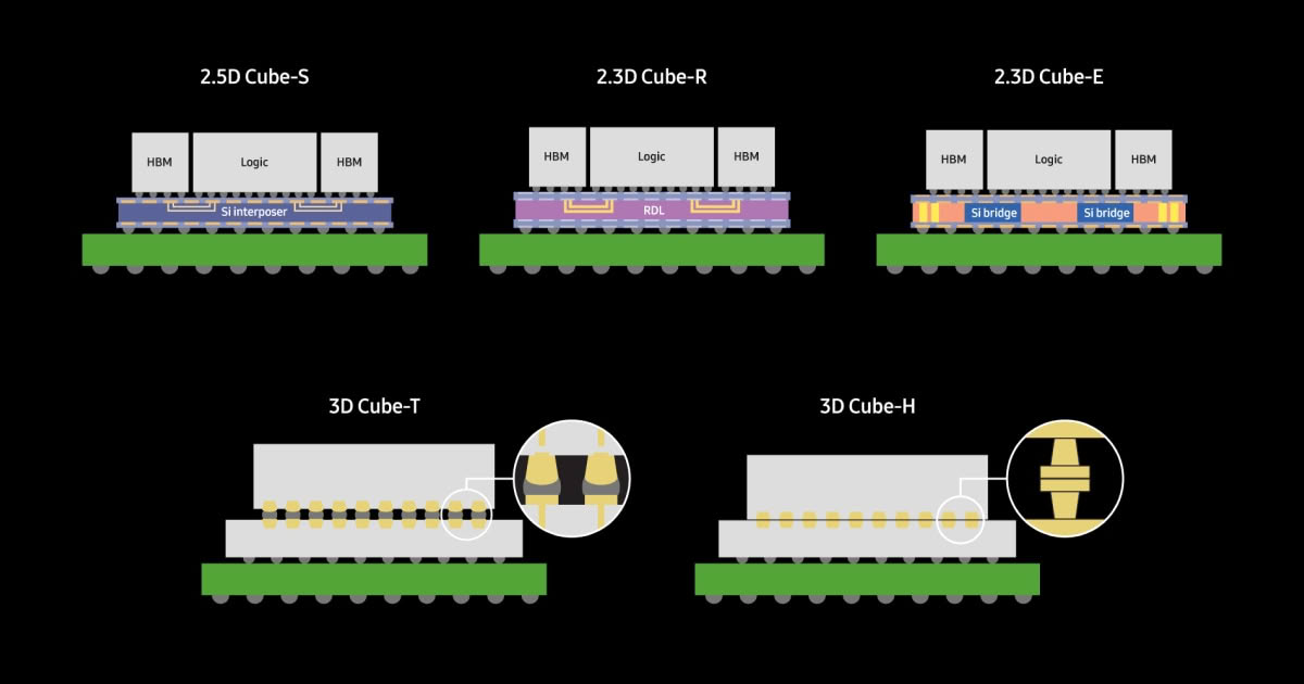
Samsung and Qualcomm have announced a partnership to develop 2.1D chip packaging technology. This collaboration focuses on creating an organic bridge solution designed to connect silicon dies, serving as an alternative to existing silicon-based interconnect methods.
The new technology utilizes organic materials, including epoxy and copper wiring, which are standard in traditional printed circuit board manufacturing. By employing redistribution layers with fine circuitry, the companies aim to achieve packaging densities comparable to Intel's EMIB approach.
Samsung plans to produce these 2.1D packages using a flip-chip ball grid array format. The technical specifications target a line width and spacing of 1.5 to 2 micrometers, with via sizes ranging between 4 and 5 micrometers for high-density integration.
The partnership sets a specific performance goal for the organic bridge architecture. The companies are aiming for a die-to-die pattern density of 500 to 1 000 connections per millimeter, leveraging manufacturing processes that resemble PCB production rather than traditional silicon fabrication.