Samsung and Qualcomm have expanded their semiconductor partnership to include 2.1D advanced packaging technology. This collaboration aims to develop high-density, high-speed chip interconnect solutions for next-generation AI and high-performance computing processors.
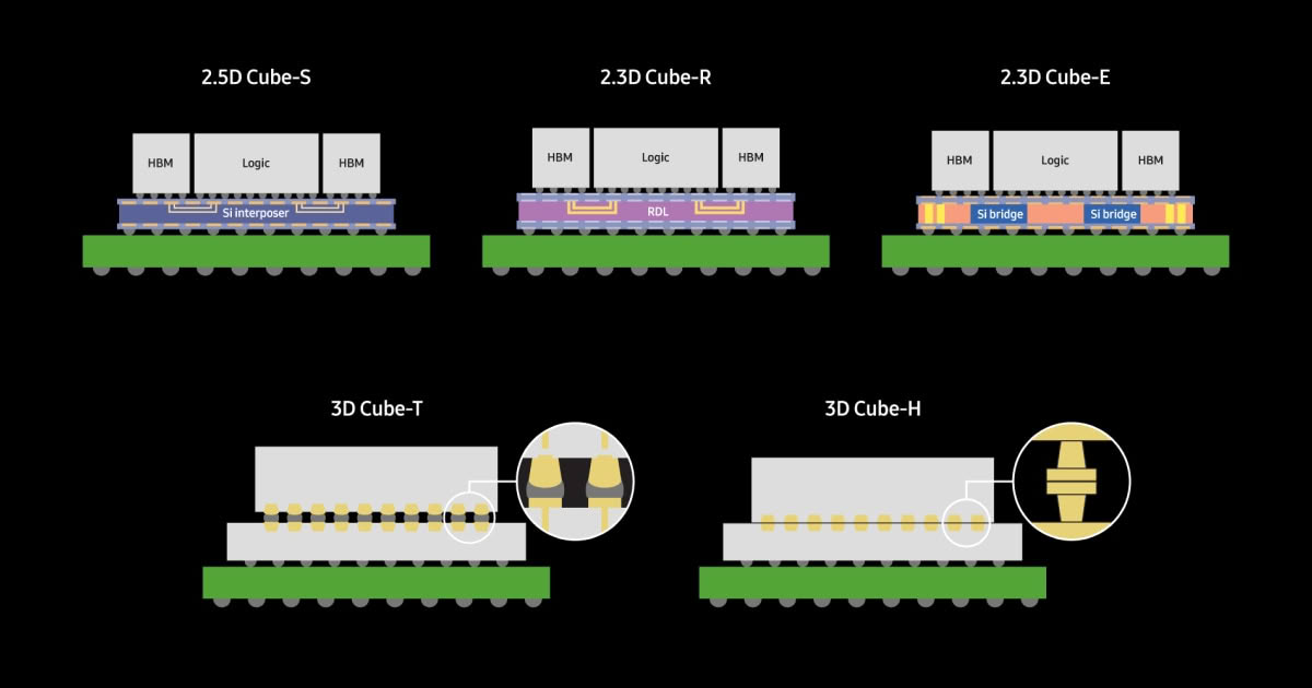
The 2.1D packaging approach eliminates the need for a silicon interposer, which is a standard component in 2.5D packaging. Instead, it utilizes high-density fine-line circuitry on the packaging substrate to connect chips directly, aiming to balance performance and production costs.
Samsung is currently developing a comprehensive AI chip ecosystem, including wafer manufacturing, HBM memory production, and advanced packaging. The company has established the Multi-Die Integration Alliance to collaborate with EDA, IP, and DSP firms to support multi-chip integration.
For Qualcomm, advanced packaging is essential for integrating compute units, NPU, and high-speed memory into SoCs for mobile and edge AI devices. This shift allows the company to move beyond simply increasing the size of individual chips to improve performance.
Samsung is also investing in other advanced packaging technologies, including 3D packaging like X-Cube and glass substrates. These efforts are part of a broader strategy to compete with TSMC in the AI chip market by offering diverse integration alternatives.