Lam Research has introduced a self-aligned complementary field-effect transistor (SA-CFET) architecture designed for nodes at 10 Å (1nm) and beyond. The architecture addresses challenges in traditional GAA nanosheet transistors, such as leakage, mobility degradation, and manufacturing process fluctuations.
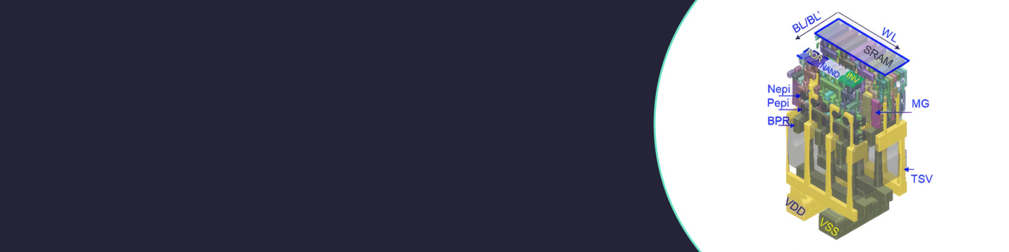
The core of the SA-CFET design relies on three self-aligned modules: SA-BPR (buried power rail), SA-CT (contact), and SA-TSV (through-silicon via). It utilizes non-metal gate-cut designs and middle-dielectric isolation (MDI) to achieve work-function separation while maintaining compatibility with N3 specifications, including a 42nm contact gate pitch and 21nm metal pitch.
Using Semiverse Solutions' digital twin process modeling, Lam Research verified the architecture for 6T SRAM and logic cells like NOT, NAND, and NOR. The 6T SRAM bit cell area reached 0.0094 μm², representing a 52.7% reduction compared to N3 and a 19% reduction compared to A7 CFET designs.
The modeling results indicate that all critical contact layers possess an overlay window of at least 10nm, with no open or short-circuit faults observed in simulations. While these results demonstrate potential process margins, Lam Research notes that the findings are based on digital twin modeling and not yet production-ready hardware.