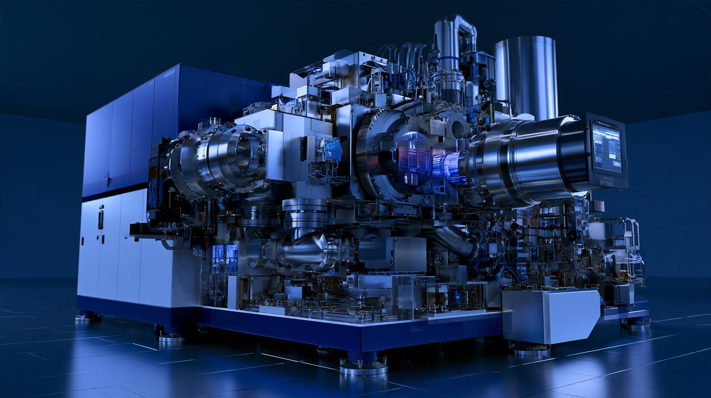
During a meeting with international media, Huawei Consumer Business Group CEO Yu Chengdong discussed the current state of China's semiconductor industry. He confirmed that Chinese research teams and industry partners are actively developing domestic EUV lithography equipment, which is essential for manufacturing advanced microchips.
Currently, mass production of Chinese chips relies on domestic DUV lithography systems. To navigate restrictions and bypass the limitations of Moore's Law, Huawei has implemented a proprietary 3D semiconductor packaging technology known as LogicFolding. This approach allows the company to increase total computing power without relying on the most advanced process nodes.
Huawei has shifted its strategy away from prioritizing the manufacturing process of individual chips. Instead, the company focuses on optimizing the device as a unified system by integrating architectural solutions, hardware, and software. This holistic method enables Huawei to maintain performance levels in its smartphones despite limited access to cutting-edge manufacturing equipment.