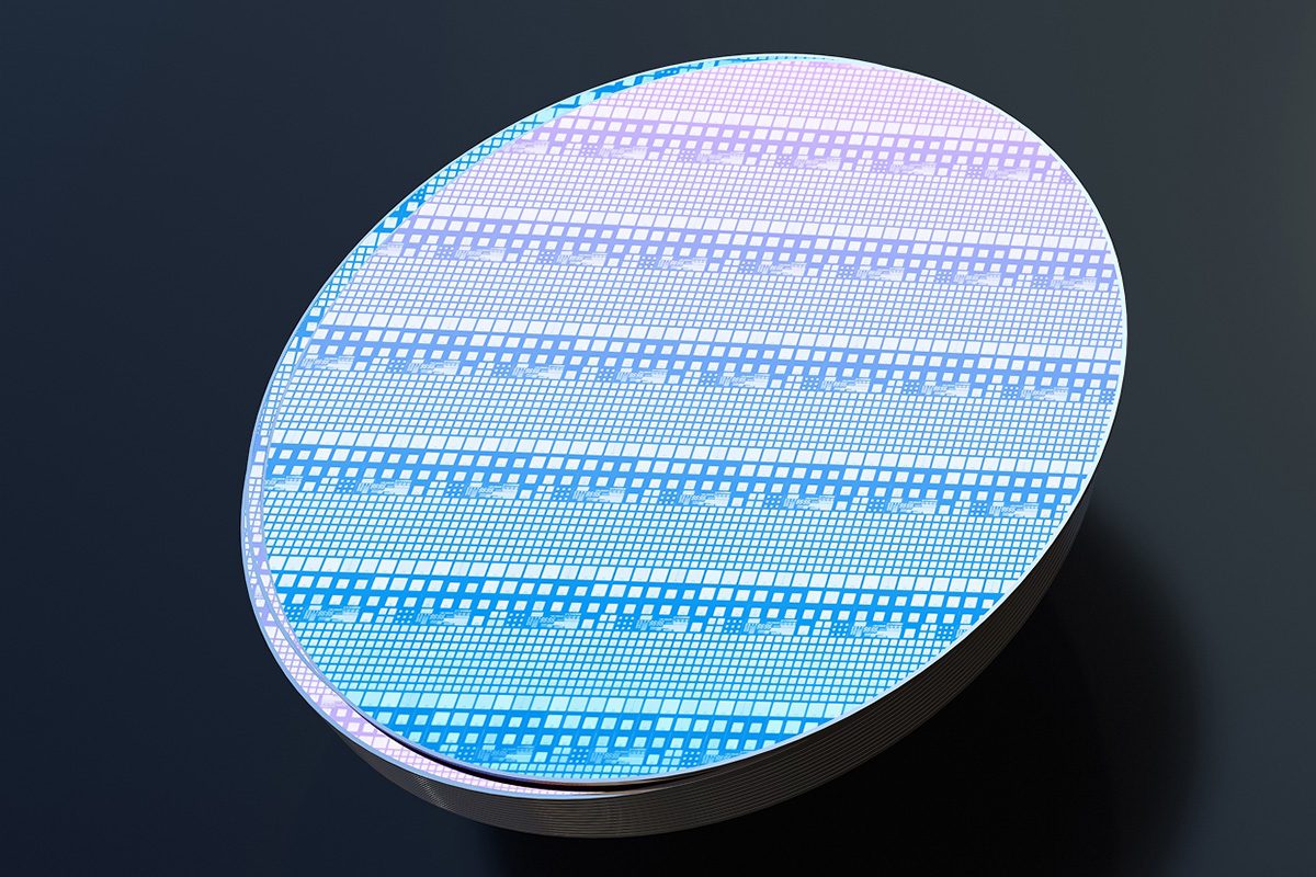
South Korean foundry DB HiTek has finished the reliability qualification for its 1,200 V silicon carbide MOSFET process using 8-inch wafers. The company claims this is the first complete 8-inch SiC foundry process flow globally, covering design, manufacturing, and testing.
The firm provides Process Design Kits for its first and second-generation technologies, with a third-generation kit expected in November 2026. These kits aim to shorten development cycles by over a year by streamlining early-stage prototyping and resource allocation.
The second-generation process features a specific on-resistance of 2.5 mΩ·cm² or less and a threshold voltage of 3 V or higher at an 18 V gate voltage. The upcoming third-generation process targets an on-resistance of 2.3 mΩ·cm² or less and a short-circuit withstand time of at least 2.5 μs.
DB HiTek intends to grant access to existing foundry clients in the third quarter of 2026, with full service availability for all customers starting in the second quarter of 2027. The company is currently preparing for volume production, which is scheduled to begin in 2027.