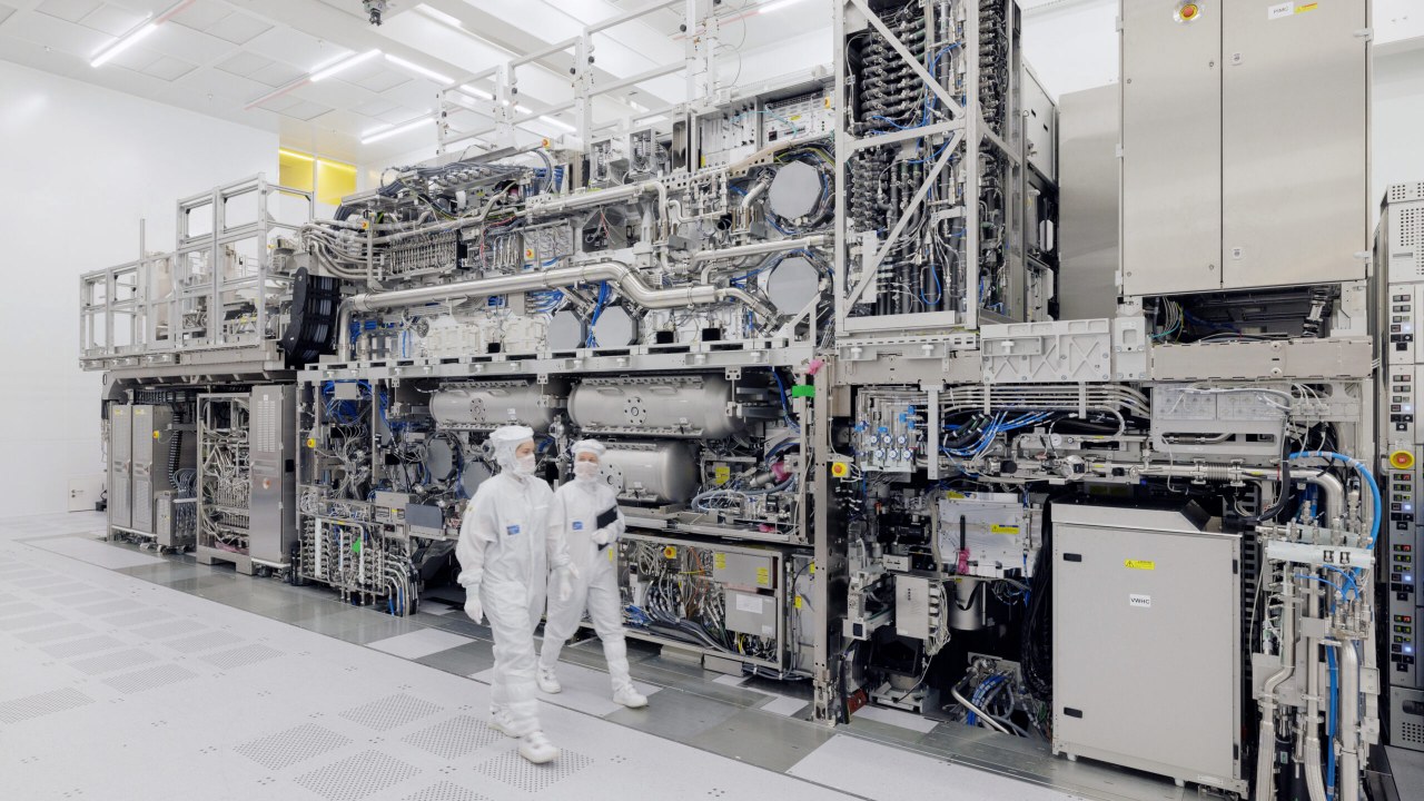
The semiconductor industry is adopting high-NA EUV lithography technology from ASML, with machines costing up to $400 million each. This equipment utilizes larger mirrors and advanced optics to create smaller, more efficient circuitry for AI data centers and consumer electronics.
Intel has already integrated high-NA EUV technology into its production lines, beginning the high-volume manufacturing of Panther Lake mobile processors in July 2026. Samsung and SK Hynix plan to implement these machines for memory chip production by 2028, while TSMC intends to use the technology for advanced client chips starting in 2030.
Major chipmakers, including Samsung, TSMC, and Intel, are collaborating with ASML to transition from 6-inch to 12-inch photomasks. According to ASML CTO Marco Pieters, this industry-wide shift is expected to increase the manufacturing productivity of high-NA EUV systems by 40 percent.
SK Hynix is currently evaluating participation in the consortium managing the transition to 12-inch photomasks. Meanwhile, ASML continues to face export restrictions regarding its advanced lithography tools to China, where local firms struggle to replicate the complex supply chain required for such systems.