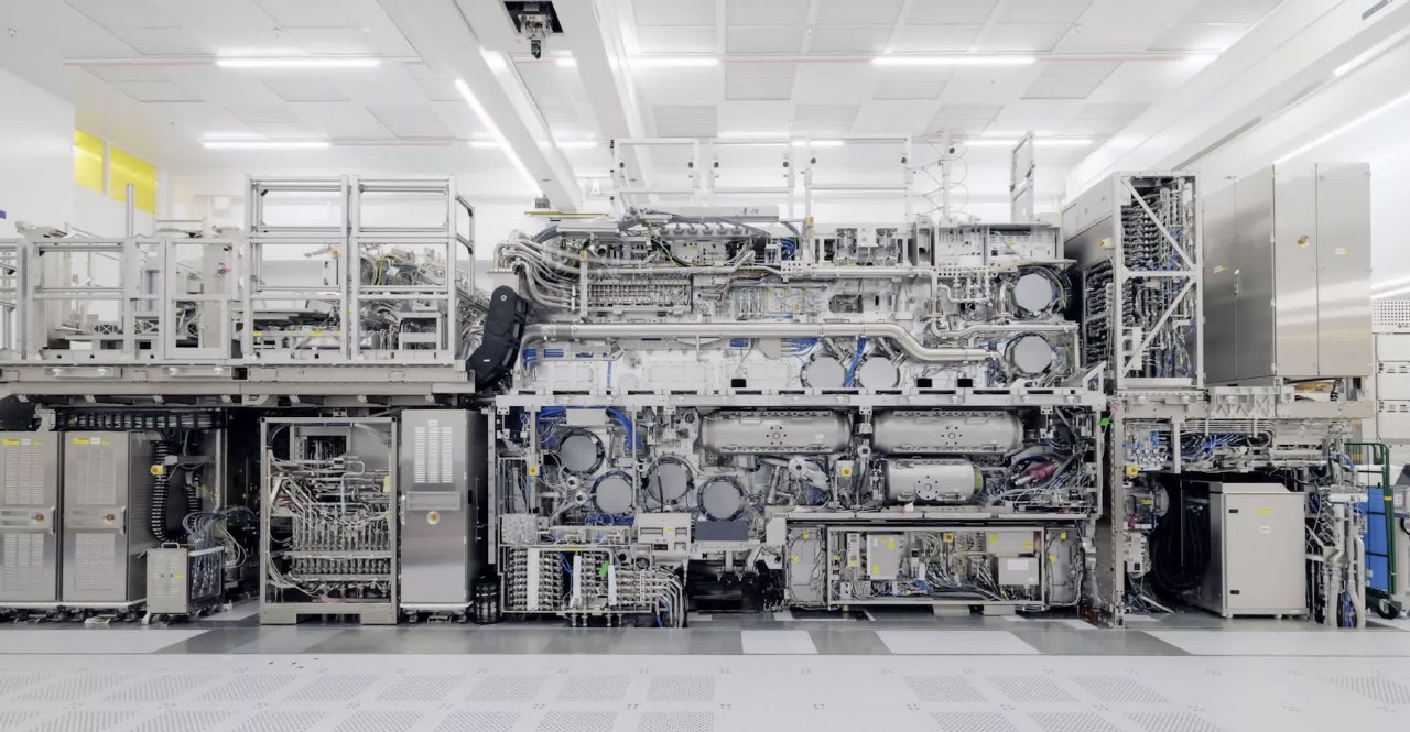
ASML is collaborating with industry partners to develop larger 12-inch photomasks for its next-generation High-NA EUV lithography systems. This adjustment aims to accommodate the increasing size of AI and data center chip designs, which currently exceed the capacity of existing EUV equipment that handles areas of approximately 800 square millimeters.
The company plans to demonstrate a pilot production line for these larger masks by 2031, with full-scale mass production targeted for 2033. According to ASML CTO Marco Pieters, this transition could improve system production efficiency by 40 percent, provided the industry coordinates effectively on the new standard.
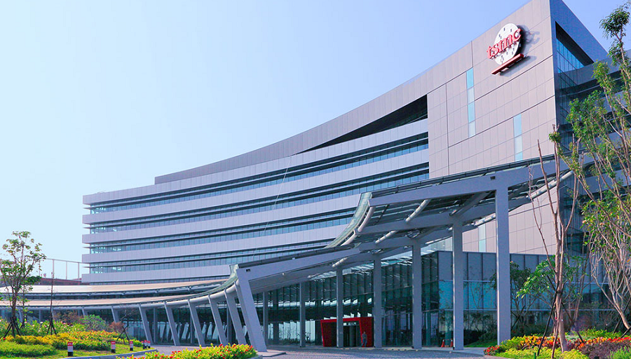
While Intel has already begun using High-NA systems for notebook chips, other major manufacturers are setting their own timelines for adoption. SK Hynix and Samsung aim to integrate High-NA EUV into DRAM mass production by 2028, while TSMC expects to implement the technology for advanced logic chip manufacturing starting in 2030.
The initiative addresses the technical limitations of current High-NA platforms, which offer higher resolution but are restricted by smaller mask sizes. By expanding the printable area, ASML intends to make the more expensive and complex High-NA equipment more viable for large-scale production of high-performance hardware.