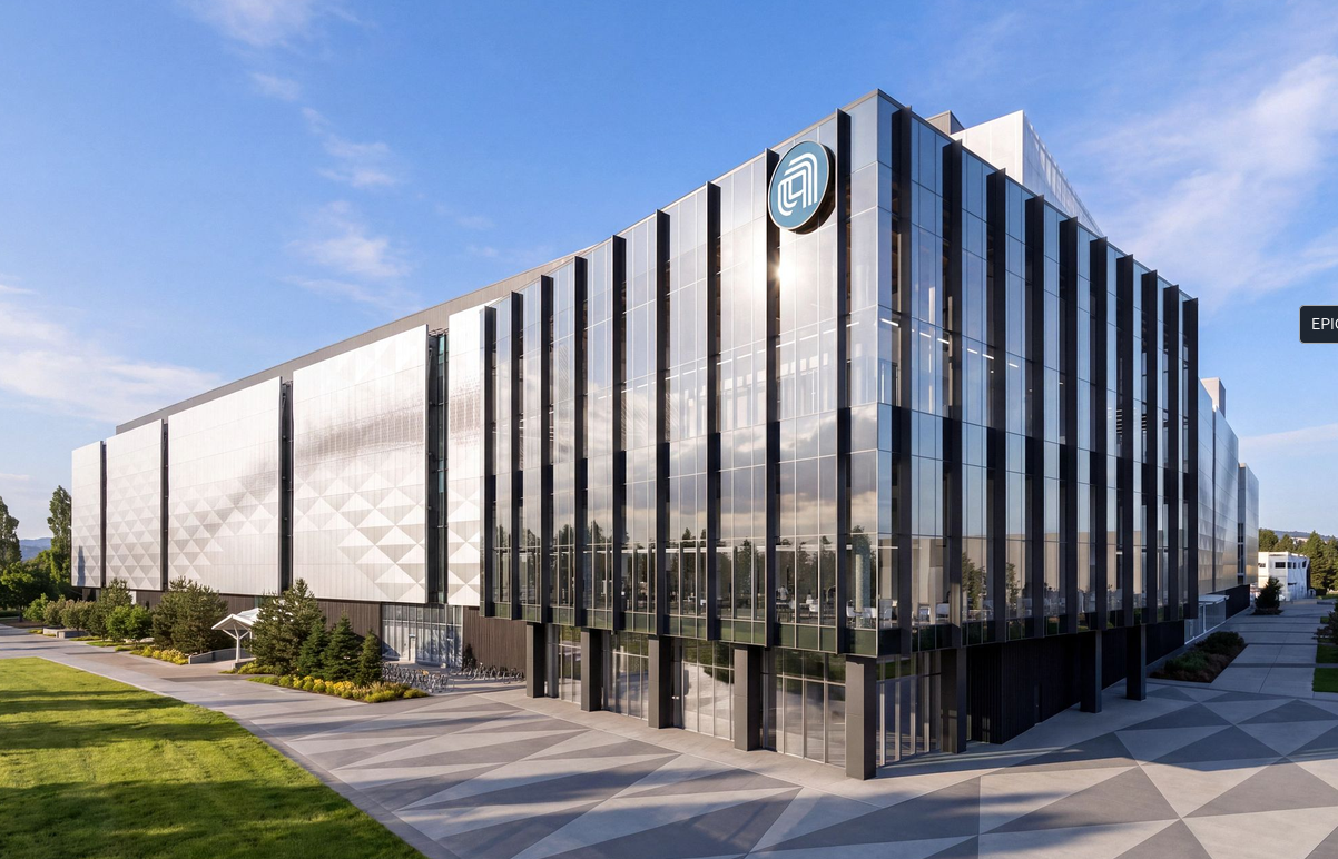
Applied Materials has launched the Equipment and Process Innovation and Commercialization Center, a $5 billion research facility located in Silicon Valley. The center spans over 600,000 square feet and includes nearly four acres of cleanroom space designed to facilitate collaborative semiconductor research.
The facility aims to reduce the research and development cycle for new chip technologies by at least 30 percent. By enabling parallel, cross-industry development, the center seeks to accelerate the time to market for innovations in 3D architectures, advanced packaging, and hybrid bonding.
Founding partners of the EPIC Center include major industry players such as Taiwan Semiconductor Manufacturing Co., Intel Corp., Samsung Electronics Co. Ltd., Micron Technology Inc., and SK hynix Inc. Additional innovation partners include Broadcom Inc. and Advantest Corp., alongside academic researchers from Stanford University, UC Berkeley, and UCLA.
According to Applied Materials CEO Gary Dickerson, the center is intended to address the increasing demands on compute performance and energy efficiency driven by artificial intelligence infrastructure. The company plans to focus on materials and process innovations that can be scaled for high-performance manufacturing.