Applied Materials and BE Semiconductor Industries (Besi) are expanding their partnership to advance hybrid bonding technology for AI hardware. The companies have collaborated since 2020, focusing on semiconductor packaging that replaces solder bumps with direct copper-to-copper connections to improve data speed and power efficiency.
In April 2025, Applied Materials acquired a 9% stake in Besi, becoming its largest shareholder. The partnership launched the Kinex die-to-wafer hybrid bonding system in October 2025. This machine integrates surface preparation, bonding, and metrology into a single process.
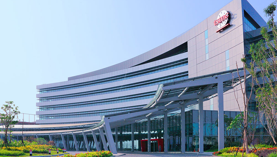
SK hynix ordered a Kinex system in March 2026 for approximately ₩20 billion to support high-bandwidth memory development. Additionally, TSMC currently uses hybrid bonding in mass production for products like AMD 3D V-Cache, while other HBM manufacturers are evaluating the technology.
Applied Materials has conducted 25 customer engagements at its Singapore Center of Excellence. Besi identifies hybrid bonding as a key component for future AI accelerators and co-packaged optics. The industry expects high-volume manufacturing for these processes to begin in 2027.