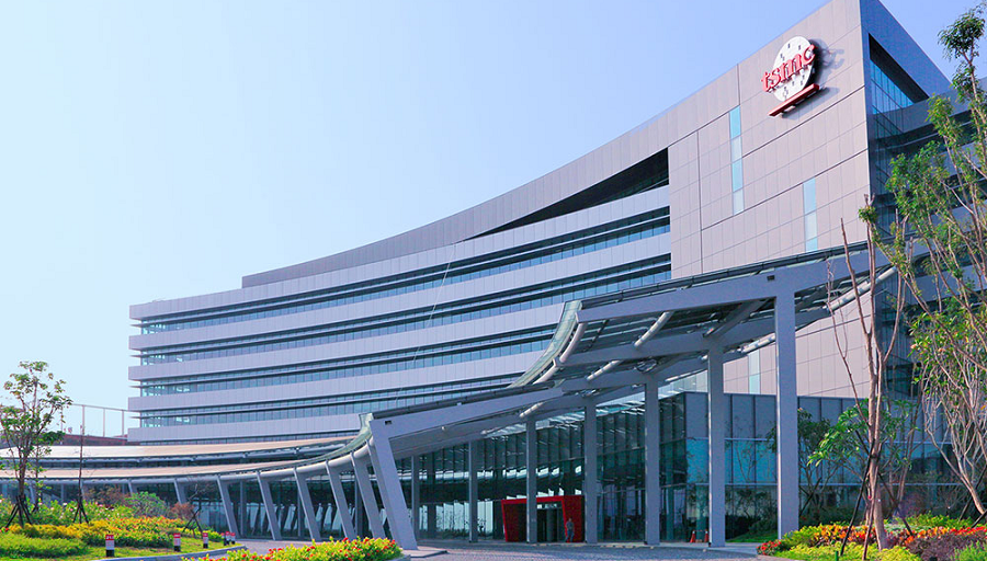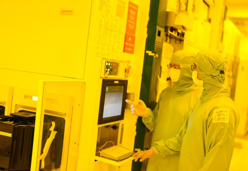
TSMC plans to begin pilot production of chips using the A14 process node in the first half of 2027. The company will utilize its Fab 20 facility in Hsinchu for initial experimental runs in the first quarter, followed by the Fab 25 site in Taichung, which is expected to begin pilot operations by the third quarter of 2027.
Mass production of A14 chips is scheduled for 2028. The company reports that early prototype yields for the A14 process have reached approximately 90 percent. Future plans for the Fab 25 site include the adoption of A13 and A12 technologies by 2029, with the latter featuring a Super Power Rail design for backside power delivery.
The A14 process will incorporate second-generation GAAFET transistors and NanoFlex Pro architecture. Compared to the N2 process, A14 is expected to offer a 20 percent increase in transistor density, along with a 10–15 percent performance boost or a 25–30 percent reduction in power consumption.
TSMC is also scaling up existing production capacities. Monthly output for 2-nm chips is projected to reach 140 000 wafers by the end of 2027, while 3-nm production is expected to exceed 200 000 wafers per month in the same period. The company intends to utilize multiple facilities, including sites in Taiwan and Arizona, for A14 manufacturing.