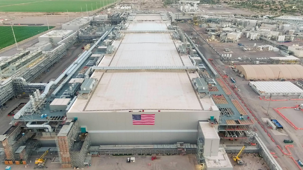


The semiconductor industry relies on TSMC for the production of advanced microchips. The company manufactures the majority of high-performance processors used in modern smartphones, computers, and graphics cards.
ASML is the sole global manufacturer of serial production equipment required for mass-producing these microchips. The process involves using extreme ultraviolet light to etch nanoscopic patterns onto silicon wafers.
The manufacturing process begins with high-purity silicon ingots, which are sliced into wafers less than 1 mm thick and 30 cm in diameter. These wafers serve as the substrate for photolithography.
Photolithography uses a light-sensitive material called photoresist. A light source projects a pattern through a mask onto the wafer, where the resist hardens or softens, allowing for the creation of complex circuit structures.
The historical development of this technology traces back to Alois Senefelder, who invented lithography in 1796. In 1826, Joseph Nicephore Niepce captured the first permanent photograph using bitumen.
Alphonse Poitevin patented photolithography in 1855, combining light-based imaging with chemical printing. By 1955, engineers at Diamond Ordnance Fuze Laboratories adapted these principles to miniaturize electronic components.