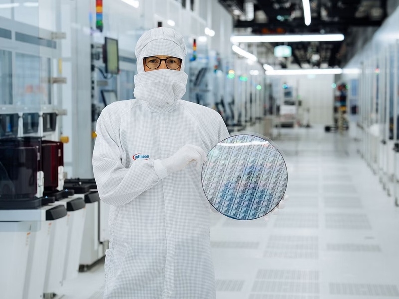


SK Hynix has commenced construction on an advanced memory packaging facility in West Lafayette, Indiana. The project represents an investment exceeding $4 billion and occupies a 133-acre site. This facility is the company's first HBM packaging operation in the United States, specifically designed to support AI applications.
The Indiana plant is scheduled to complete its cleanroom by October 2028, with volume production of next-generation HBM4E chips projected for the second half of 2029. Once fully operational, the site is expected to generate approximately 1,000 jobs. The project has secured up to $458 million in funding through the CHIPS Act.
Simultaneously, SK Hynix is evaluating plans for a dedicated NAND flash fabrication plant in the United States, with upstate New York identified as a potential location as of September 2026. However, as of late October 2026, no final investment decision has been reached regarding the site, costs, or timeline for this facility.
The development of the NAND facility is linked to regulatory considerations regarding equipment shipments to the company's existing plant in Dalian, China. SK Hynix CEO Kwak Noh-Jung has indicated that the global memory chip shortage may persist until the end of 2030, noting that these US projects are unlikely to provide immediate relief.