

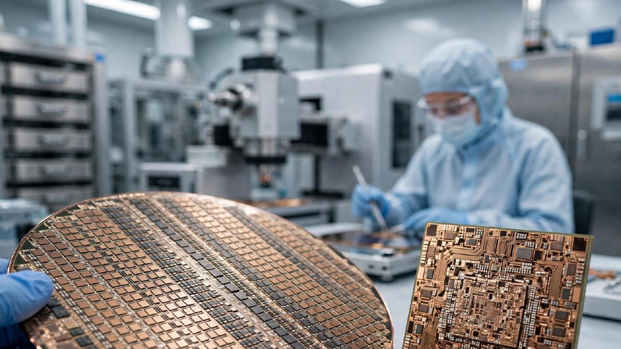
Samsung Electronics is reportedly considering utilizing TSMC's 3nm process technology to manufacture base dies for specialized NVHBM memory chips intended for Nvidia. This strategic move follows a proposal from Nvidia to standardize the base dies across its memory suppliers, including Samsung, SK Hynix, and Micron, using a unified manufacturing process for sixth-generation DRAM.
The base die in high-bandwidth memory architecture acts as the critical interface between memory layers and other system components. In the context of NVHBM, the role of this component is increasingly significant, necessitating higher production standards. Reports suggest that Samsung has acknowledged these requirements while still evaluating the feasibility of producing these components in-house.
Industry analyst firm TrendForce has noted that Samsung is exploring a dual-sourcing strategy for its HBM production. This approach would allow the company to choose between internal manufacturing and outsourcing to TSMC based on specific client requirements. However, as of October 18, no formal agreements between Samsung and TSMC regarding this production scheme have been officially confirmed.