Qualcomm has officially entered into a licensing agreement with Huawei to incorporate various technologies into its product portfolio. The deal, which is estimated to be worth $6.9 billion upon completion, covers areas including computing, artificial intelligence, and networking.
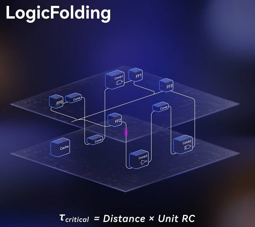
A key component of the agreement is the inclusion of Huawei's LogicFolding silicon design. This technology involves stacking silicon vertically across two sheets, which reduces the distance between compute elements. Huawei reports that this method increases transistor density by 55% and improves power efficiency by 41%.
Huawei developed LogicFolding as a workaround for limited access to EUV lithography, utilizing DUV machines instead. The company projects that by 2031, its domestic production using this technique will reach a transistor density equivalent to a 1.4 nm node.
For Qualcomm, which maintains access to advanced lithography, the integration of LogicFolding offers a pathway to potentially exceed Moore's Law. By applying this stacking method to its own silicon, the company aims to achieve significant gains in both transistor density and power efficiency.