
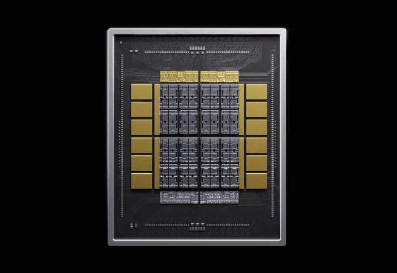
Nvidia has coordinated a collaboration between TSMC and Samsung to develop NVHBM memory. Under this arrangement, Samsung will utilize 3nm base dies manufactured by TSMC for the initial production of this memory type.
The NVHBM architecture shifts auxiliary functions away from the GPU, allowing for more compute units. This design reduces the physical interface block area by 60 percent compared to standard HBM, while increasing bandwidth by up to 30 percent and lowering power consumption by 15 percent.
Nvidia selected TSMC for 3nm base die production because the foundry achieves a yield rate exceeding 90 percent. In contrast, Samsung currently struggles to exceed 60 percent yield for the same process, making TSMC the primary supplier for Nvidia's requirements.
UBS forecasts a 91 percent increase in HBM demand next year, with supply projected to cover only 90 percent of market needs. While Samsung relies on TSMC for current NVHBM production, it is simultaneously working to certify its own 2nm process for future independent manufacturing.
Beyond NVHBM, the two companies are collaborating on advanced chip packaging technologies. Samsung intends to continue manufacturing base dies for standard HBM and custom solutions for other clients using its own internal production facilities.