Intel is actively preparing for the mass production of its 14A process node. According to supply chain reports, the company plans to establish a monthly production capacity of approximately 6,000 wafers by the end of 2027. This node is positioned as a key element in Intel's advanced foundry roadmap following the 18A process.
The 14A process is expected to utilize High-NA EUV lithography technology. While the projected capacity is limited, it is intended to support initial customer adoption, technical validation, and the manufacturing of high-value products. Intel is currently engaged in equipment deployment and customer verification processes for this node.
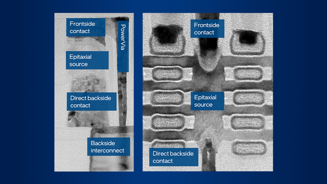
Simultaneously, Intel's 18A process has reportedly reached a yield of approximately 80%. This milestone is considered critical for the company's foundry business, as it indicates technical feasibility for mass production. The 18A node incorporates RibbonFET transistor architecture and PowerVia backside power delivery.
Intel aims to leverage these process nodes to compete with industry rivals like TSMC and Samsung. The success of the 18A mass production and the subsequent implementation of the 14A node are central to the company's 'five nodes in four years' strategy. Market analysts remain cautious, citing potential risks from equipment delivery and competition.