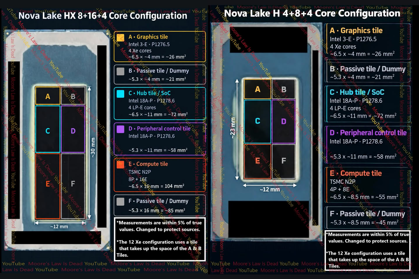
The first images of Intel Nova Lake processor dies have surfaced, revealing details about the H and HX mobile variants. The Nova Lake-H chip features a 4+8+4 configuration, while the Nova Lake-HX model utilizes an 8+16+4 setup.
The larger HX die measures 30 by 12 millimeters, resulting in a total area of 360 square millimeters. The smaller H die measures 23 by 12 millimeters, covering 276 square millimeters. Both chips consist of six tiles, though two of these are dummy silicon pieces used for structural integrity.
The architecture includes identical GPU tiles with four Xe cores, along with shared Hub and I/O chiplets. These components are manufactured using the 18A-P process, while the GPU tile utilizes the Intel 3 process. The processor chiplets are produced by TSMC using the N2P node.
Intel plans to release the Nova Lake series early next year under the Core Ultra 4000 branding, marking another shift in the company's product naming convention.