
Fujifilm is investing $18 million to expand its semiconductor material production facility in Mesa, Arizona. The company plans to launch the new manufacturing capacity in 2027 to meet the rising demand from high-performance logic and memory chip manufacturers.
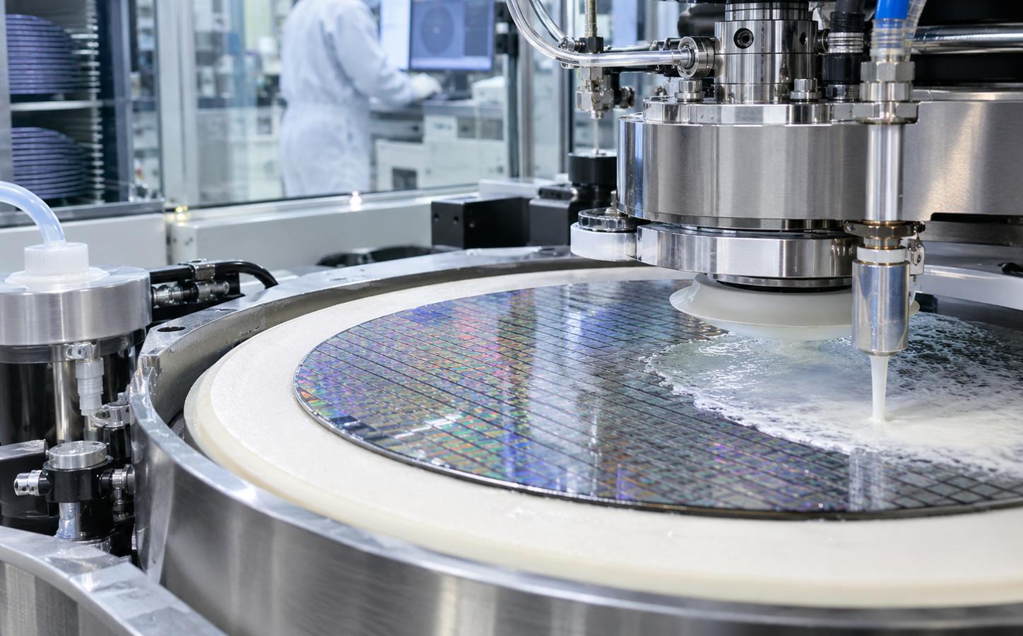
The expansion focuses on chemical mechanical planarization (CMP) slurries, which are essential for leveling semiconductor wafers. The facility will prioritize the production of slurries for copper interconnects, while also supporting materials for FEOL, MOL, and BEOL manufacturing stages.
The project aims to support hybrid bonding technology, which requires extremely flat and clean surfaces to create dense electrical contacts between chips. This process is critical for advanced chip packaging, as it improves integration density and reduces signal transmission distances.
The Mesa site already hosts an international research center for CMP materials. By integrating research and industrial production, Fujifilm aims to ensure consistent quality and volume for its specialized chemical compositions used in semiconductor fabrication.
Fujifilm has not disclosed specific production capacity increases, job creation figures, or the names of client companies. Despite the relatively modest investment compared to industry-wide capital expenditures, the project targets a key bottleneck in advanced chip manufacturing.