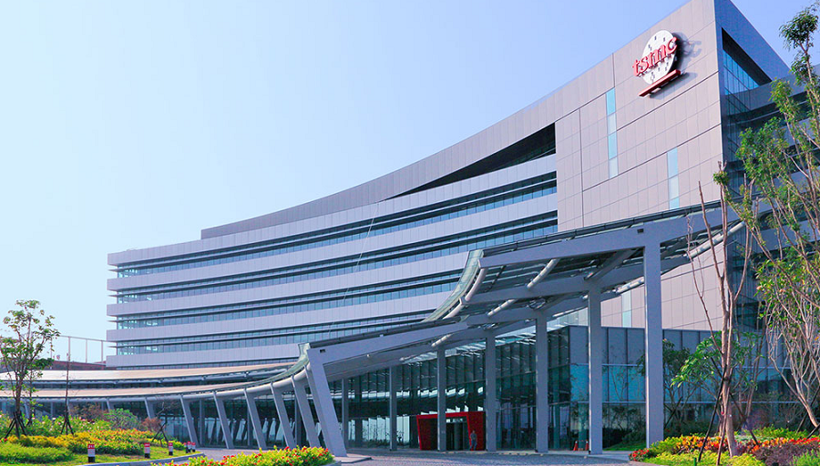
Analysts at Kurnal Insights estimate the cost of a 300-mm wafer using TSMC N3 technology at $20,000, or $0.283 per square millimeter. For the N2 process, the estimated cost rises to $30,000, or $0.424 per square millimeter. These figures represent nominal wafer-area prices and exclude factors like yield and dicing.
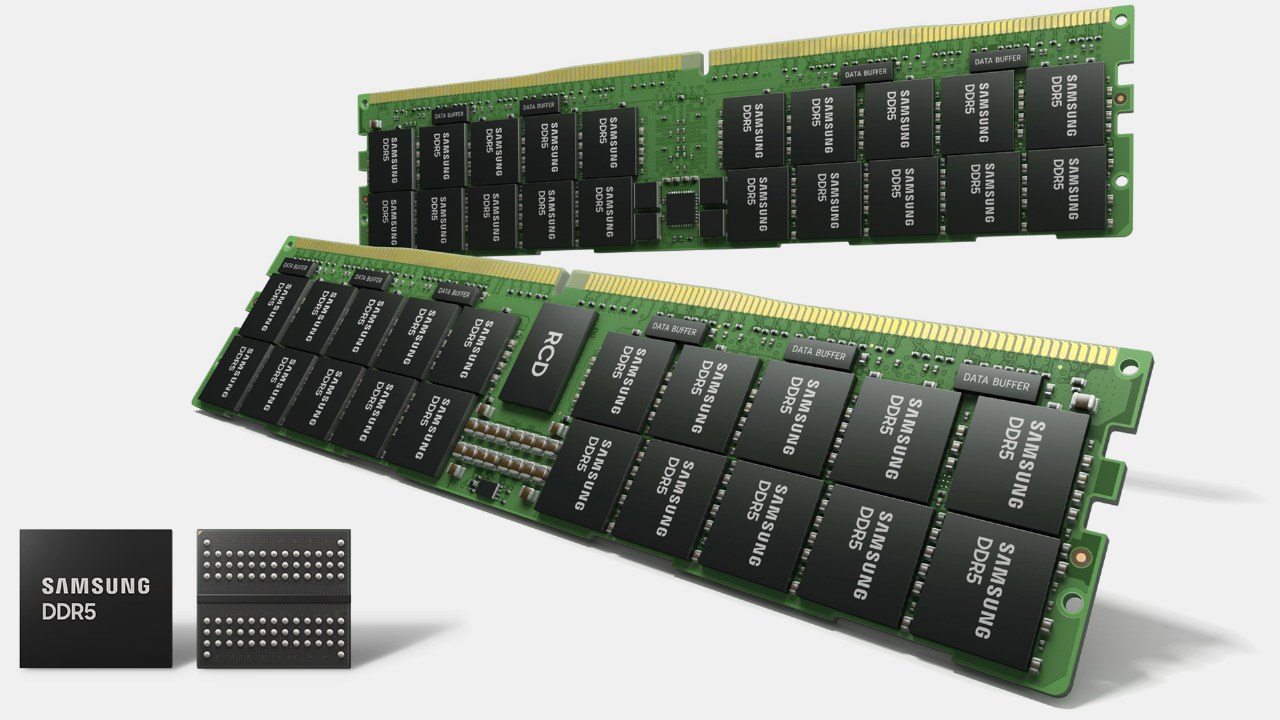
In contrast, DRAM value is calculated based on bit density and market pricing. At a price of $1.50 per Gb, 1b generation DRAM reaches a value of $0.654 per square millimeter. This exceeds the nominal cost of an N2 logic wafer, highlighting the significant revenue potential for memory manufacturers driven by current demand.
Market data from DRAMeXchange confirms these trends, with 16Gb DDR5 eTT chips trading at an average of $24.80, or $1.55 per Gb. At this rate, the value of 1b DRAM silicon rises to approximately $0.676 per square millimeter, which is 3% higher than previous estimates.
Experts note that these comparisons are not direct, as they contrast contract manufacturing costs for logic chips with spot market values for memory. Factors such as packaging costs, contract volumes, and the difference between spot and bulk pricing mean that actual profitability for companies like Micron, Samsung, and SK hynix may vary.