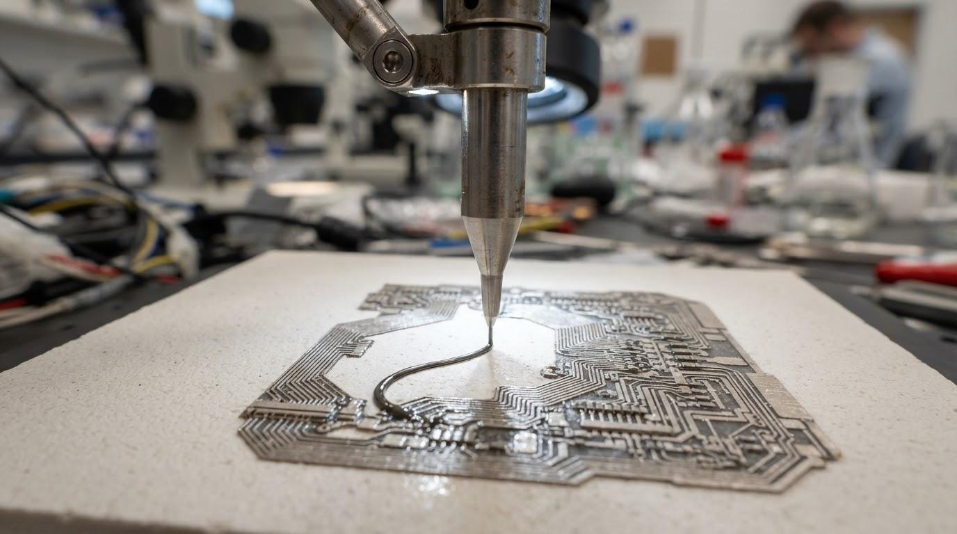
Researchers at TUSUR University have upgraded a printer designed for manufacturing printed circuit boards and integrated circuits. The system applies conductive pastes directly to substrates, eliminating the need for traditional stencils. The project is being developed by the Additive laboratory in collaboration with an industrial partner.
The initial prototype underwent testing at a production facility in 2024. Following feedback, the team focused on improving positioning accuracy and usability. A key challenge involves multi-layer printing, where the nozzle must account for surface height variations of 10–15 microns on films that are approximately 30 microns thick.
To enhance precision, the team is developing a non-contact distance measurement system, utilizing technology adapted from a genomic printer project. Additionally, the printer now features a camera for machine vision. Developers have tested a defect recognition algorithm on static images and are currently working to adapt it for real-time video streams.
This direct printing method is intended for prototyping and small-batch electronics production. By replacing physical stencils with digital models, the technology aims to reduce both the time and costs associated with developing new electronic devices.