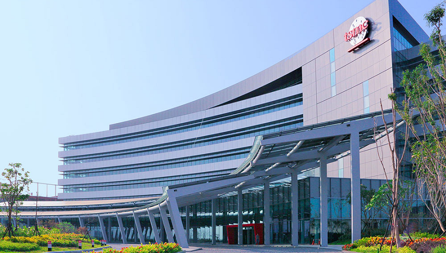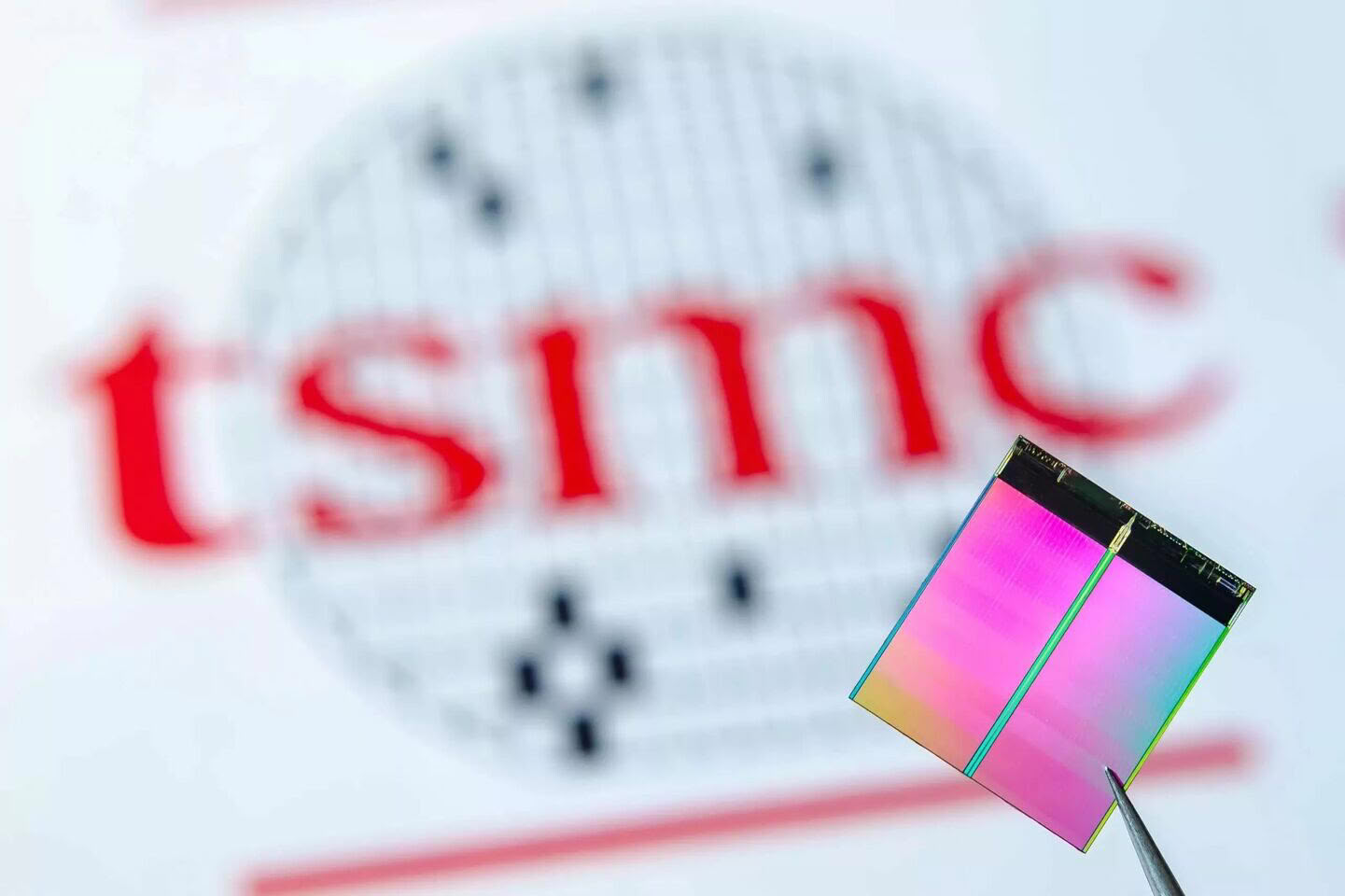
TSMC has initiated pilot production for its A14 semiconductor node, which features 1.4 nm technology. The process is currently underway at the company's Fab 20 facility in Hsinchu Science Park and Fab 25 in Central Taiwan Science Park. These runs aim to evaluate node viability and allow clients to test design performance within the production environment.
The development of the A14 node is currently exceeding initial expectations, potentially allowing for an accelerated timeline. If the pilot phase remains stable, TSMC plans to move to risk production in 2027, with full-scale high-volume manufacturing slated for 2028. The company notes that the schedule could shift forward by several months if no significant technical issues emerge next year.
The A14 process provides notable performance improvements over the N2 2 nm node. It offers up to 15% higher speeds at equivalent power levels or up to 30% power reduction at the same frequency. Additionally, TSMC reports a 20% increase in logic density. The company intends to launch mass production at its headquarters in Taiwan, maintaining a competitive edge over Intel and Samsung.