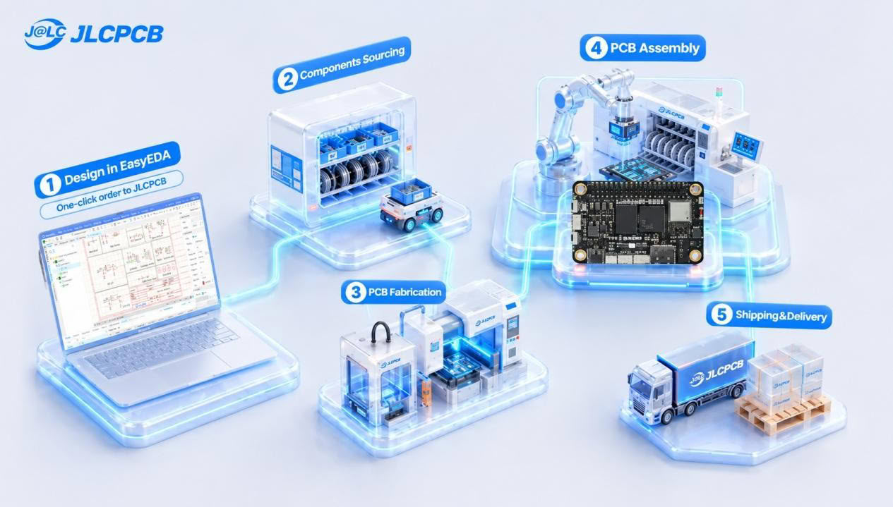
EasyEDA and JLCPCB offer a unified workflow for hardware prototyping, integrating design, component sourcing, fabrication, and assembly. This approach aims to minimize manual data transfers and coordination issues between development stages.
The EasyEDA platform provides browser-based schematic and PCB design tools, supporting project collaboration, version control, and imports from Altium Designer and KiCad. Users can choose between Standard and Pro versions based on project complexity.
JLCPCB integrates its component library directly into the design environment, allowing engineers to verify availability during the layout phase. This helps prevent design rework caused by component shortages or manufacturing constraints.
The manufacturing service supports multilayer PCB fabrication ranging from 1 to 32 layers with various surface finishes. It handles SMT, through-hole, and mixed-technology assemblies, including fine-pitch components like 0201, 01005, BGA, and QFN.
Quality control processes include SPI, AOI, and X-ray inspection to detect defects in hidden solder joints. The service allows for small-batch production, facilitating iterative testing and faster validation cycles for hardware development.