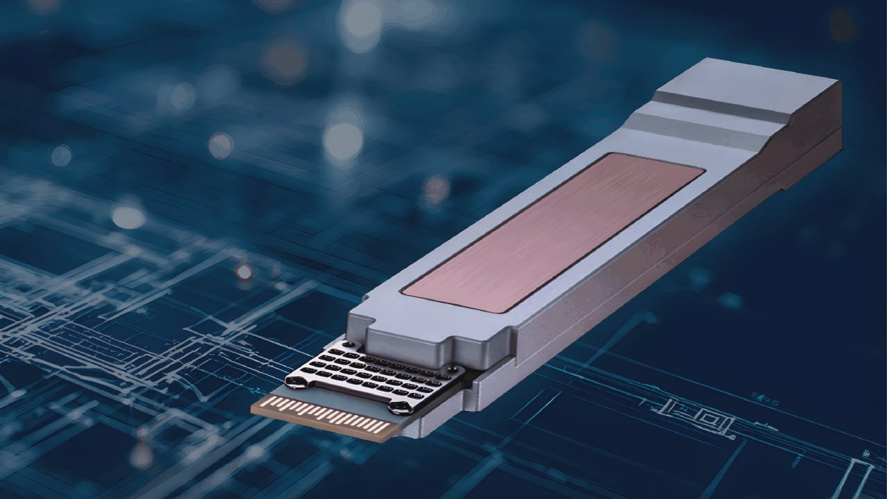
SK Hynix unveiled its H-TPU (Hynix Transaction Processing Unit) architecture on October 12, 2026, at the ISOCC conference in Incheon, South Korea. The company designed this specialized processor to address performance bottlenecks in AI data centers where traditional general-purpose CPUs have reached their limits in SSD control.
The H-TPU architecture replaces a single large CPU with dozens of small, programmable TPU clusters. By breaking down control functions into specific units, the system ensures that only modules relevant to a task, such as data writing, remain active. Unused modules switch to a low-power mode to minimize energy consumption.
Technical specifications indicate that the H-TPU occupies only 1/25 of the area of a standard CPU core, accounting for approximately 4% of the total CPU footprint. Furthermore, the architecture consumes only 2.5% of the power required by traditional CPUs, utilizing a simplified four-stage pipeline that excludes superscalar and out-of-order execution.
SK Hynix intends to integrate H-TPU technology into its NAND product lines, specifically for next-generation enterprise SSD (eSSD) controllers. The company also plans to incorporate this technology into its upcoming AI storage architecture, known as Storage Next.
The company expects significant synergy between H-TPU-based controller innovations and its new High Bandwidth Flash (HBF) memory, which is scheduled for release next year.