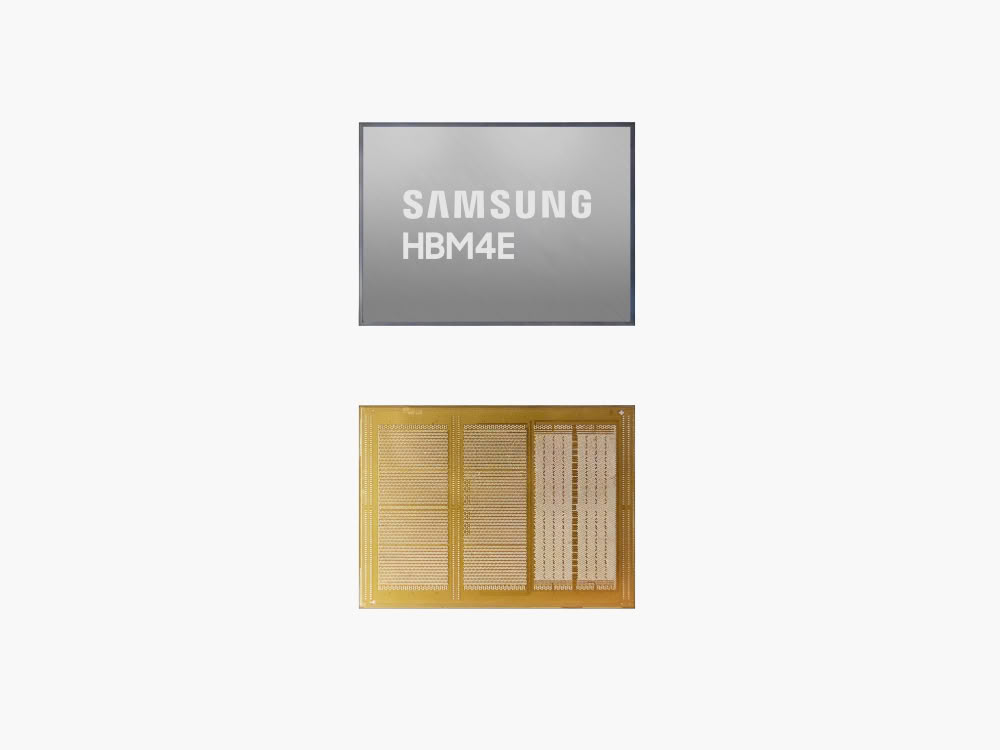
Samsung is scaling up its high-bandwidth memory production to meet rising demand for AI accelerators. The company plans to double its manufacturing capacity for HBM4 and HBM4E chips by 2027. Projections indicate that output will rise from approximately 20 000 wafers per month in 2026 to 50 000 wafers per month in 2027.
These estimates are based on the procurement of glass carriers, which are essential for stabilizing thin DRAM wafers during the packaging process. Each wafer requires one glass carrier, allowing for precise production tracking. Samsung currently utilizes these components to manage the complex stacking requirements inherent in modern HBM architectures.
Total HBM output, encompassing older generations like HBM3 and HBM3E, is projected to reach 250 000 wafers next year, up from 180 000 wafers in 2024. Notably, 80% of this capacity will be allocated to HBM4 and HBM4E. Mass production of HBM4 using the 10 nm-class 1c node began in February, with customer samples for HBM4E expected by mid-2026.