

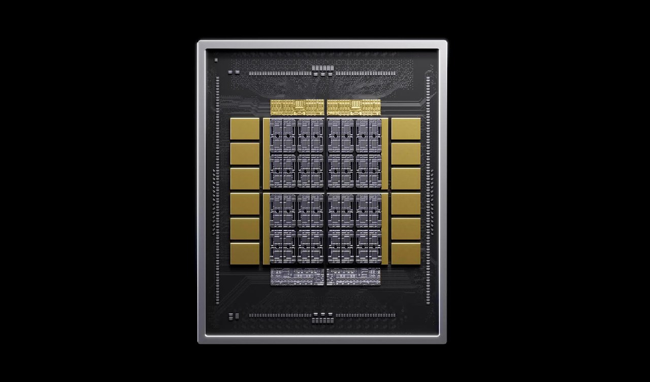
Samsung has entered into a partnership with TSMC to produce base dies for NVIDIA's new NVHBM memory standard. This collaboration is necessary because NVIDIA requires the base dies to be manufactured using TSMC's 3 nm process node, which is optimized for its intellectual property.
The NVHBM standard integrates a controller directly into the 3D HBM stack. According to NVIDIA, this architecture provides up to 30 percent higher memory bandwidth and 15 percent lower power consumption compared to the standard HBM4E. Additionally, it offers up to 25 percent more usable compute die area.
Despite having its own 3 nm production capabilities, Samsung will outsource the base die manufacturing to TSMC. For the memory components, Samsung plans to continue utilizing its proprietary sixth-generation 10 nm processes, which are standard for its HBM production line.