
Samsung Foundry plans to launch its second-generation 8nm process, 8LPU+, by the end of this year. Compared to the previous 8LPU generation, the new platform delivers a 12% performance increase, a 15% reduction in power consumption, and an approximately 8% decrease in logic area.
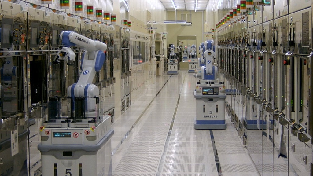
The 8LPU+ process utilizes existing deep ultraviolet (DUV) lithography production lines that have already completed depreciation. This strategy allows Samsung to avoid the high costs associated with extreme ultraviolet (EUV) lithography equipment, which is currently limited in supply and expensive to procure.
The process is specifically designed for automotive and industrial applications, including AI microcontrollers (MCU) and zonal control units (ZCU). These sectors prioritize long-term supply stability, operating temperature ranges, and cost-effectiveness over peak computing power.
To support miniaturization, the 8LPU+ platform integrates 3.3V planar I/O devices, reducing I/O area by approximately 10%. Additionally, the process features ultra-low leakage SRAM and high-threshold voltage devices to minimize standby power consumption in idle states.
The embedded magnetic memory (eMRAM) used in the process meets Automotive Grade 1 (AG1) standards. It features a cell area of 0.017 square micrometers and a storage density of approximately 20Mb/mm², enabling more compact controller chip designs.