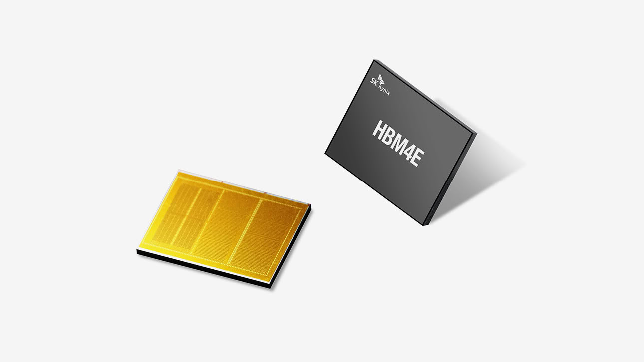
SK Hynix is reportedly facing development challenges with hybrid bonding technology, a critical advancement for next-generation High Bandwidth Memory (HBM). Industry sources indicate that while Samsung has already provided samples of HBM chips utilizing this technology to customers, SK Hynix has yet to begin sample production.
Hybrid bonding replaces traditional micro-bumps by directly connecting metal interconnects between chips. This approach enables 3D stacking of multiple chips or entire wafers, which reduces signal latency, improves energy efficiency, and allows for thinner packaging. It is considered essential for future HBM products with 16 or more layers.
Despite its potential, hybrid bonding presents significant manufacturing hurdles. The process requires extreme precision in wafer flatness, surface cleanliness, and alignment, making yield and cost control difficult. Industry experts suggest that large-scale adoption may not occur until the HBM4E or HBM5 generations.
SK Hynix currently leads the HBM market with approximately 50 percent of global shipments for HBM3E and HBM4 products, while Samsung holds about 33 percent. However, SK Hynix's market share has declined from a previous high of 64 percent, as Samsung continues to expand its presence in the sector.