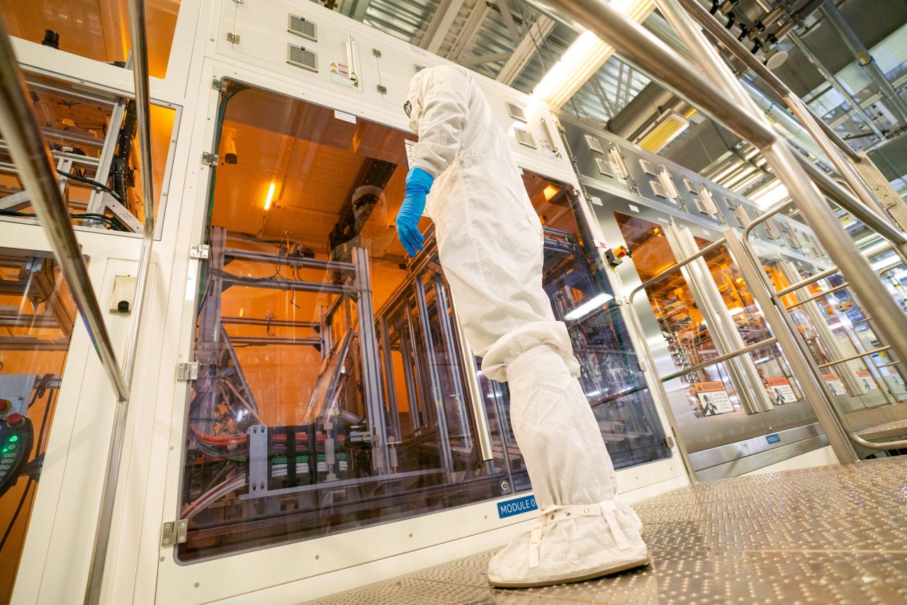
Samsung Electronics has joined a consortium led by ASML to develop next-generation semiconductor manufacturing technology. The partnership focuses on advancing 12-inch photomask technology to replace the long-standing 6-inch photomask format.
The companies aim to increase fab production efficiency and reduce chip manufacturing costs, specifically to meet the rising demand for AI chips.
Samsung also plans to integrate ASML's High NA EUV lithography technology into the mass production of DRAM by 2028.