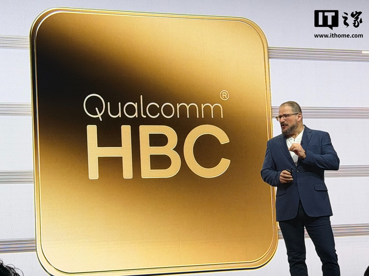
At the 2026 Snapdragon Summit held on September 22, Qualcomm announced the integration of High Bandwidth Compute (HBC) architecture into its Snapdragon chips. Initially introduced at the Investor Day in June 2026 for data center hardware, this technology is now transitioning to mobile processors.
HBC is a near-memory computing architecture that positions the compute chip directly beneath stacked LPDDR DRAM. By utilizing 3D integration and through-silicon vias (TSV), the design minimizes the distance data must travel. This approach aims to address the memory wall bottleneck that currently limits AI inference performance on mobile devices.
By moving computation closer to memory, the architecture reduces the need for constant data movement between the processor and memory. This shift is expected to lower latency and decrease power consumption. Consequently, future smartphones equipped with HBC-integrated chips will be capable of running larger on-device AI models and more complex features locally.
While HBC does not increase total memory capacity, it improves effective bandwidth and performance per watt. These enhancements allow mobile devices to handle models with higher parameter counts and longer context windows, overcoming current limitations where NPU computing power is restricted by data transfer speeds.