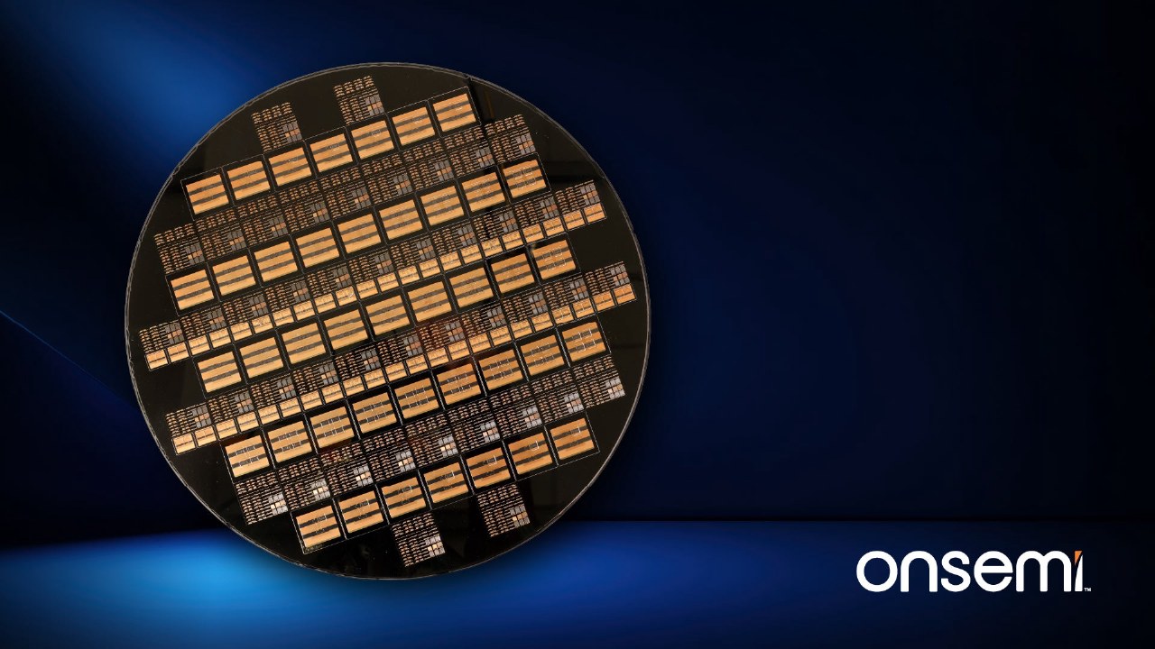
Onsemi has introduced its new Embedded Power Platform (EPP), which utilizes 12-inch silicon wafers as packaging carriers. This architecture allows for the integration of multiple dies into a single device, achieving a power density that is 3 to 5 times higher than current market solutions.
The EPP platform supports the integration of silicon, silicon carbide, and gallium nitride technologies. It enables the embedding of various components, including field-effect transistors, drivers, and controllers, within a single package while facilitating co-design, co-simulation, and co-optimization of electrical, mechanical, and thermal factors.
Early testing of a solid-state circuit breaker using the EPP technology demonstrated a 50% reduction in size and a 20% decrease in operating temperature. For electric vehicle traction inverters, the platform offers up to a 4-fold increase in power density and a 15% reduction in power losses.
Onsemi plans to begin providing samples of the EPP to customers in 2026. The company is currently collaborating with Subaru to evaluate the platform's potential for supporting future electric vehicle architectures.