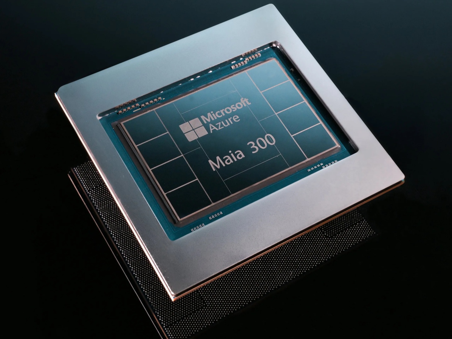
Microsoft has officially unveiled the Maia 300 AI chip, which is manufactured using TSMC's N2P 2-nanometer process. The chip features a multi-chiplet design that integrates dedicated memory and I/O chiplets. The company plans to begin deployment of the new hardware in 2027.
The Maia 300 delivers an FP4 performance of 13.8 PFLOPS and an FP8 performance of 6.9 PFLOPS. Its power consumption is rated at 950W, an increase from the 750W rating of the previous Maia 200 model. The architecture includes 8 sets of HBM4 memory, providing a total capacity of 288GB and a bandwidth of 18TB/s.
For large-scale operations, the chip supports a bidirectional interconnect bandwidth of 3.2TB/s and utilizes a two-layer network architecture based on Ethernet. A single rack can house 96 Maia 300 units, allowing for the creation of clusters that include up to 12 000 accelerators.