
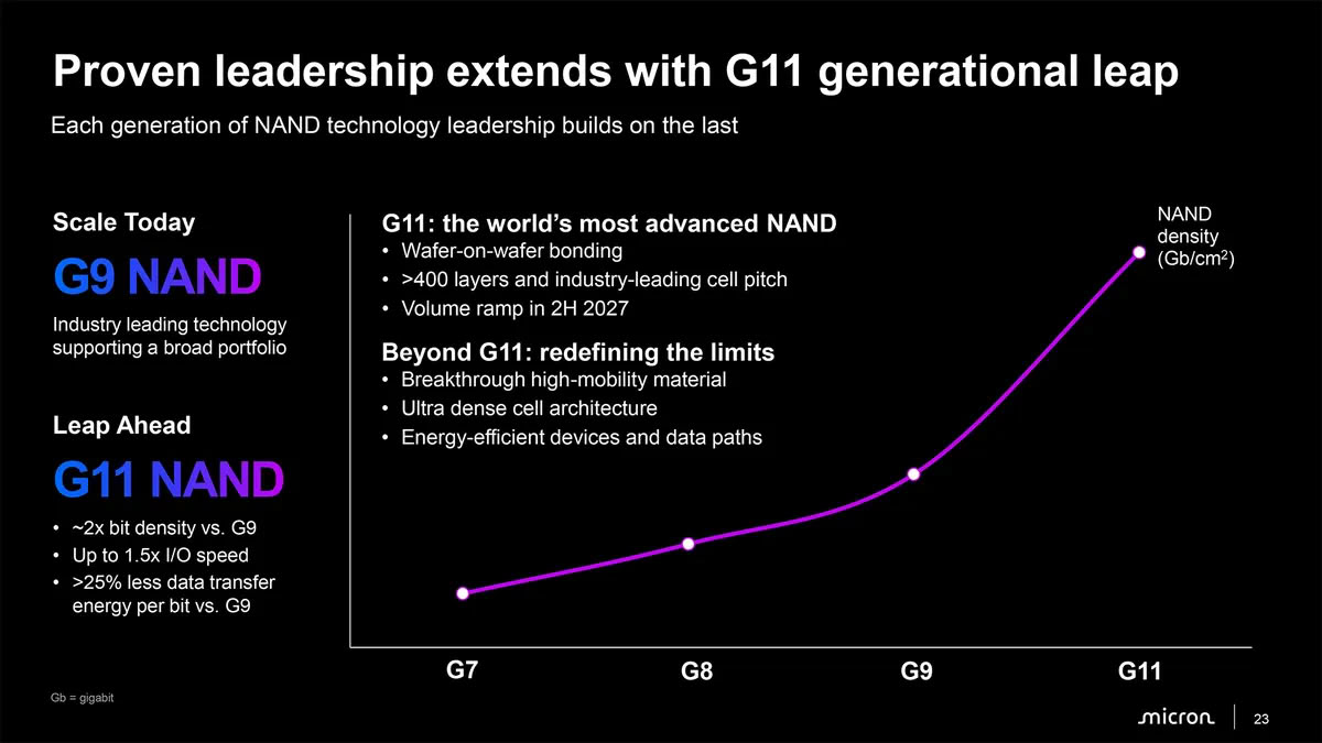
Micron is currently transitioning to its G11 NAND Flash technology, which marks the company's first move into advanced 3D stacking. This development follows the successful deployment of the G9 generation, which currently utilizes over 200 layers of scaling across the company's existing product portfolio.
To overcome the physical limitations of existing scaling methods, Micron will implement wafer-on-wafer 3D stacking. This approach involves splitting the production process into two distinct components: one wafer dedicated to memory cells and another containing peripheral logic circuits. These are then joined using hybrid bonding.
The hybrid bonding process utilizes embedded metal bumps that fuse together, creating a permanent connection between the two silicon chips. This method allows for the stacking of multiple dies or entire wafers, effectively doubling the capacity of the resulting NAND storage modules.
Micron expects to begin shipping its 400-layer NAND products in the second half of 2027. This strategy aligns the company with the manufacturing techniques previously established by YMTC, which has utilized similar Xtacking technology for its own 3D stacked NAND production.