Kepler Computing has exited stealth mode after seven years of development. The startup is introducing a memory technology that serves as an alternative to HBM by utilizing ferroelectric RAM, or FeRAM. The company employs a 3D stacking technique and new materials to maintain standard HBM capacity while lowering manufacturing costs.
The startup avoids the need for advanced semiconductor nodes by using mature manufacturing processes. In a collaboration with GlobalFoundries, Kepler converted a standard 28 nm facility into a memory fab in eight months. This timeline is notably faster than the 24 months typically required for traditional DRAM production.
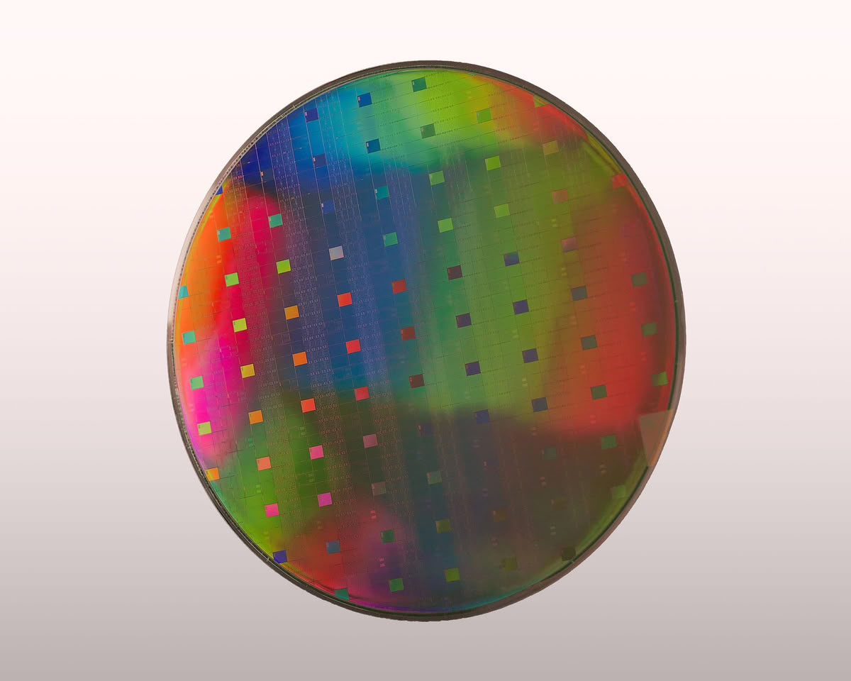
To date, the company has processed approximately 2 000 wafers using its new DRAM technology. The first samples of the HBM alternative are scheduled for release later this year. Kepler plans to initiate full-scale volume manufacturing at the GlobalFoundries facility in Singapore next year, with production in the United States expected to follow in 2028.
The development process involved 35 iterations of composites to reach a scalable design. By utilizing existing mature nodes, the company aims to manufacture both HBM and SRAM without relying on EUV lithography. This approach is intended to address the current memory crisis through more efficient and cost-effective production methods.