Kepler Computing, a startup founded in 2018, has developed a new 3D memory architecture and a proprietary material that allows for increased density in HBM and SRAM chips without the need for expensive EUV lithography. The technology is designed to be deployed on existing semiconductor manufacturing facilities, potentially bypassing the need for building new, costly production plants.
The company has raised $468 million from investors including Intel Capital, AMD Ventures, and GlobalFoundries. Additionally, the US Department of Commerce has pledged up to $245 million for the development of high-performance memory for AI systems. GlobalFoundries, which also invested $50 million, is serving as the primary manufacturing partner for the project.
By utilizing ferroelectric materials and a new composite, Kepler claims to achieve SRAM density comparable to 2nm and 3nm processes. The startup successfully retrofitted a semiconductor facility in eight months, compared to the industry standard of two years. The company estimates these costs are significantly lower than the $20–40 billion required to build new factories.
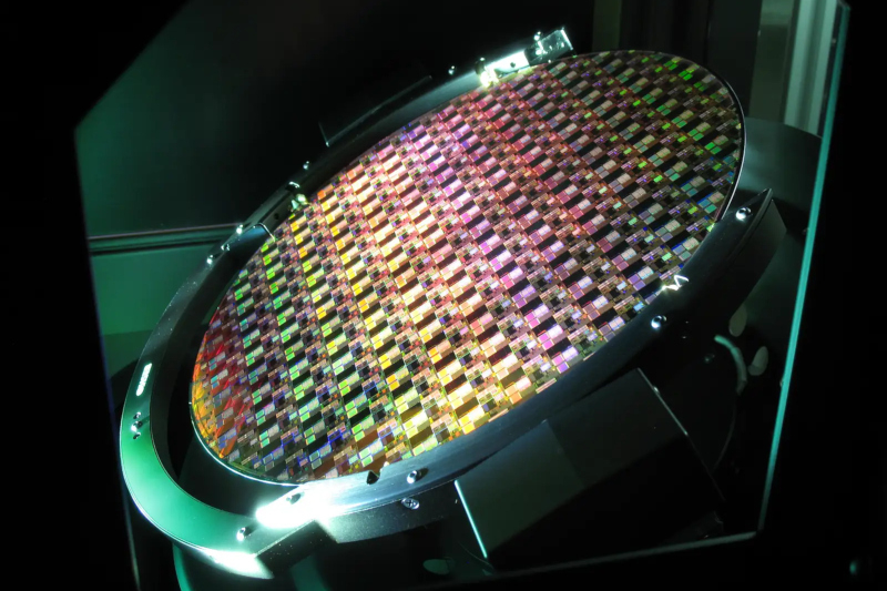
The technology currently faces challenges, such as the presence of iron in the composite material, which acts as a contaminant for standard production lines. To date, the process has been tested on 2,000 wafers. Kepler plans to release initial HBM samples this year, scale production in Singapore in 2027, and potentially begin manufacturing in the United States by 2028.