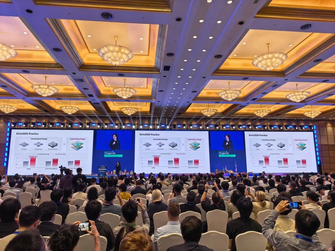
Huawei has officially introduced the 'Tau' (τ) law, a new evolution path for semiconductor technology. This approach shifts the focus from traditional geometric scaling to time-based optimization. The company aims to improve performance by reducing signal propagation delays and optimizing data flow efficiency across various hardware levels.
Richard Yu, Chairman of the Terminal BG, confirmed that Huawei has successfully designed and mass-produced 381 types of Tau-based chips. These components are currently utilized in smartphones, AI applications, general computing, networking, and smart automotive systems. The strategy prioritizes minimizing wait times and data travel paths within the architecture.
The core of this methodology involves 'Logic Folding' and multi-level optimization, covering devices, circuits, chips, and systems. By optimizing transistor interconnects and implementing the Lingqu bus for unified memory addressing, Huawei seeks to enhance transistor density and energy efficiency. These technical advancements aim to reduce end-to-end execution time.
Looking ahead, Huawei projects significant progress in its semiconductor roadmap. By 2031, the company expects that high-end chips developed under the Tau law will achieve a transistor density equivalent to that of 1.4-nanometer process technology. This development marks a strategic shift in how the company approaches future hardware scaling limitations.