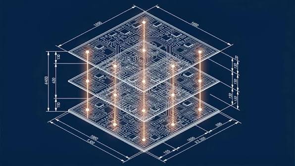
Huawei has introduced the LogicFolding 3D chip architecture, which rearranges logic units vertically to shorten signal paths and reduce the number of clock buffers. Data from the company indicates that this design can reduce the number of clock buffers in a processing module from approximately 43,600 to 19,000, a decrease of over 50%.
The architecture is based on the Tau Scaling Law, which prioritizes signal propagation time and interconnect distance over traditional transistor scaling. Huawei reports that key signal paths can be shortened by up to 70%, with average signal path lengths reduced by approximately 20%. This approach aims to improve performance and energy efficiency without relying solely on advanced lithography.
Industry experts express concerns regarding thermal management, as vertical stacking increases power density within a limited volume. High-power modules like CPUs, GPUs, and NPUs create localized heat spots, which may force the chip to throttle performance. Huawei is currently exploring solutions such as diamond heat dissipation layers and micro-fluidic cooling channels to address these thermal challenges.
Recent teardowns of Huawei's latest processors confirm the use of two vertically stacked chip layers connected via copper-to-copper hybrid bonding. While this structure improves signal efficiency, it introduces manufacturing complexities, including thermal stress and yield management. The company is now transitioning this technology from research to commercial production in its Kirin processors.