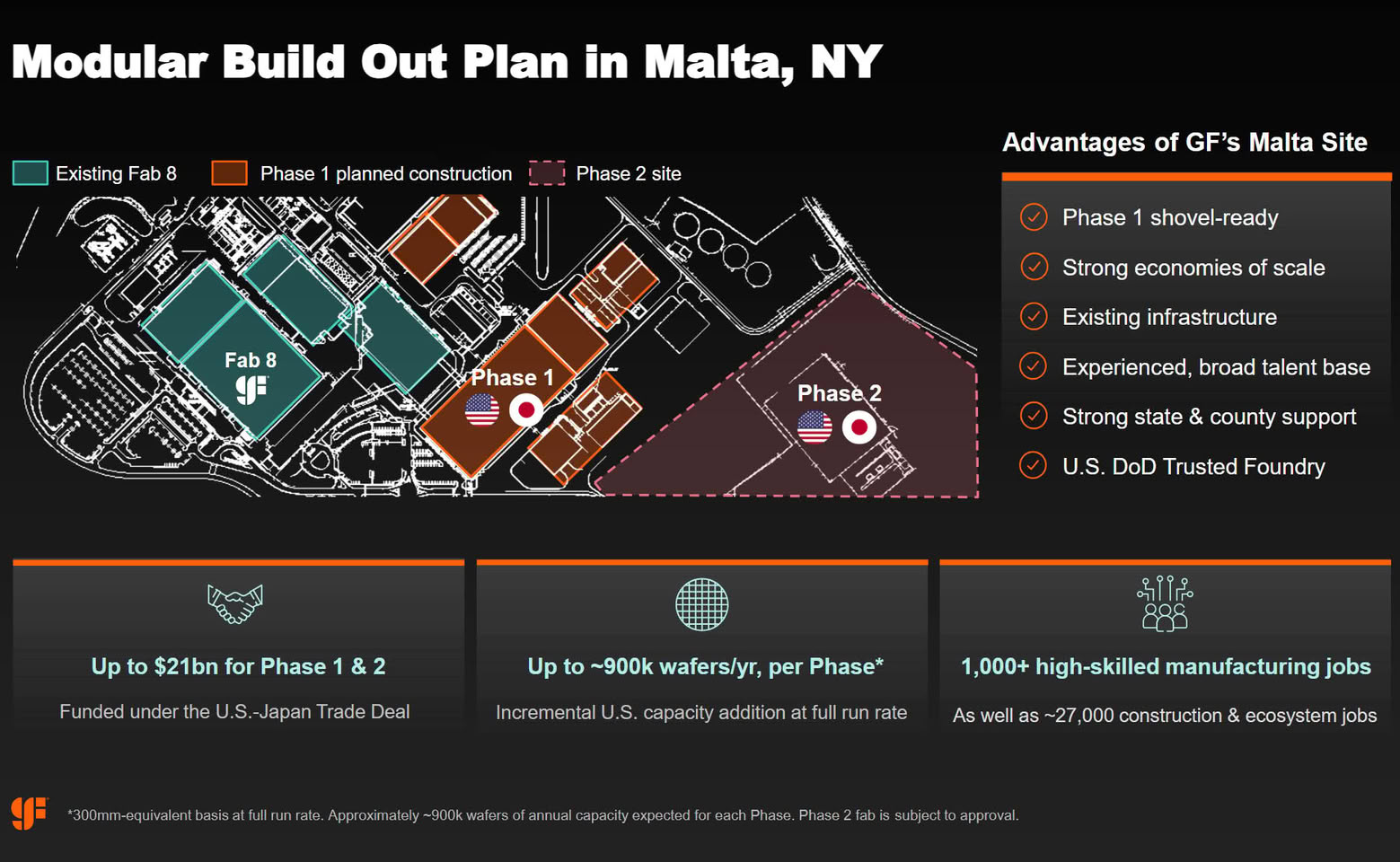
GlobalFoundries will manage two upcoming semiconductor facilities in Malta, New York, as part of a U.S.-Japan initiative backed by $21 billion in total funding. The first 300 mm fab requires an initial investment of $10 billion, with construction starting this year and production slated for 2029. The second facility will also receive $10 billion in funding at a later date.
Each plant is expected to reach an annual output of 900 000 wafers once fully operational. Baseline capacity for the first fab is projected for 2031-2032, while the second is expected to reach this milestone in 2033. The expansion supports the company's focus on advanced packaging and semiconductor manufacturing, including a partnership with AMD for co-packaged optics on Instinct MI500 accelerators by 2027.
The company is also scaling its 7 nm-class FDX Fusion technology, with mass production scheduled for 2028 at its Dresden site. Additionally, GlobalFoundries reached an agreement with the U.S. Department of Commerce to reallocate $955 million from its CHIPS and Science Act award toward silicon photonics, SiGe, and advanced packaging in New York and Vermont. The U.S. government will receive a 4% equity stake as part of this deal.
GlobalFoundries currently holds the fifth position among the world's top ten foundries, trailing TSMC, Samsung, SMIC, and UMC.