
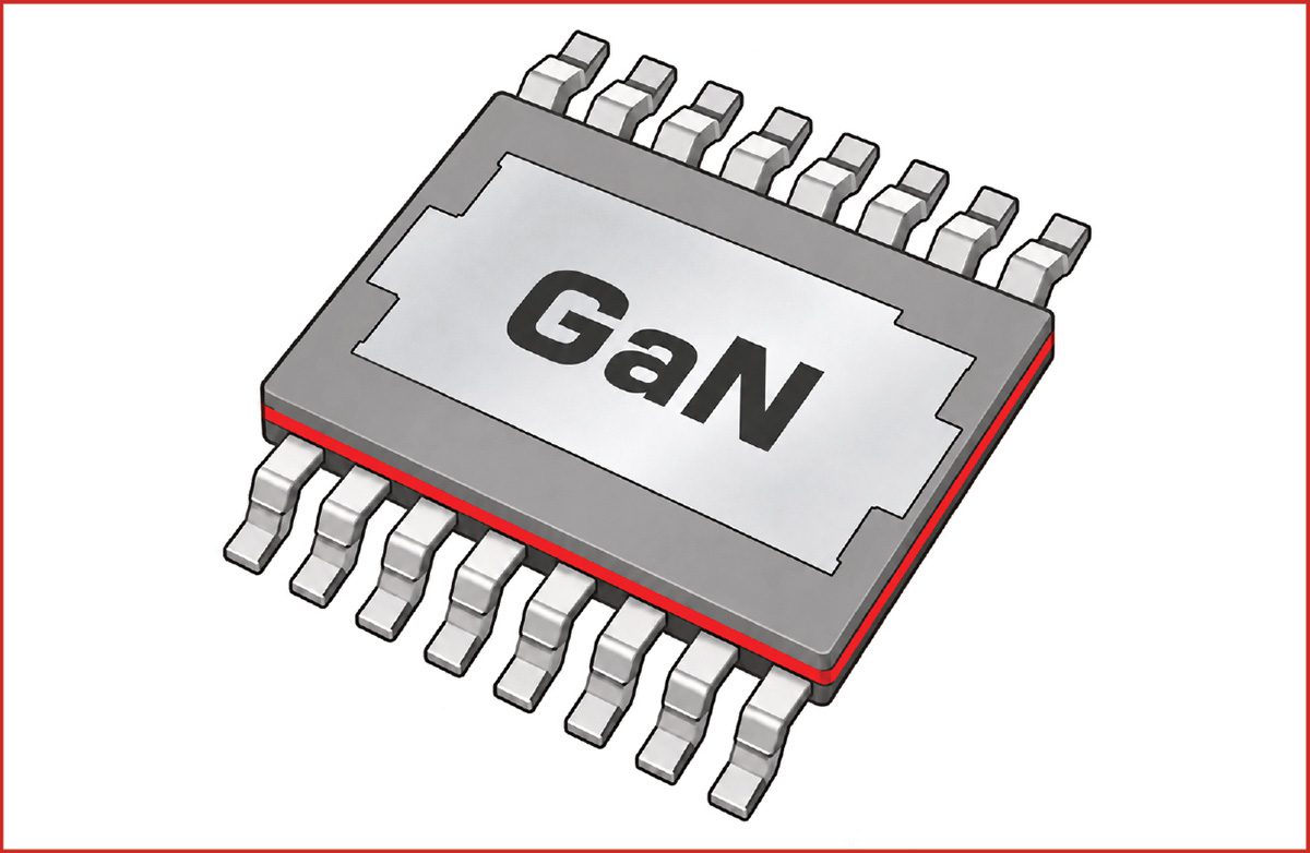
Wide band-gap semiconductors like SiC and GaN are increasingly replacing silicon due to lower power losses at high frequencies. While SiC MOSFETs are widely adopted in EV applications due to their thermal stability and standardized packaging, GaN switches offer distinct physical advantages, including smaller die sizes for specific voltage ratings and superior electron mobility.
GaN technology enables significantly lower on-resistance and faster switching speeds compared to silicon and SiC. However, current market availability for GaN is largely limited to 650 V, whereas SiC components are readily available at 1200 V or higher. GaN devices also exhibit unique characteristics, such as current collapse and specific gate drive requirements that vary by manufacturer.
Designing with GaN requires careful management of loop inductances, often necessitating specialized packages like BGA or LGA to minimize stray inductance. Because GaN switches lack the standardized behavior of silicon counterparts, engineers must consult specific manufacturer datasheets for gate drive configurations to avoid issues like spurious turn-on.
While GaN is highly effective for applications like onboard chargers and DC/DC converters where size and weight reduction are critical, it is less suitable for traction inverters. The technology's lower pulse current capability and extremely high switching speeds can create challenges in high-power motor drive environments.