
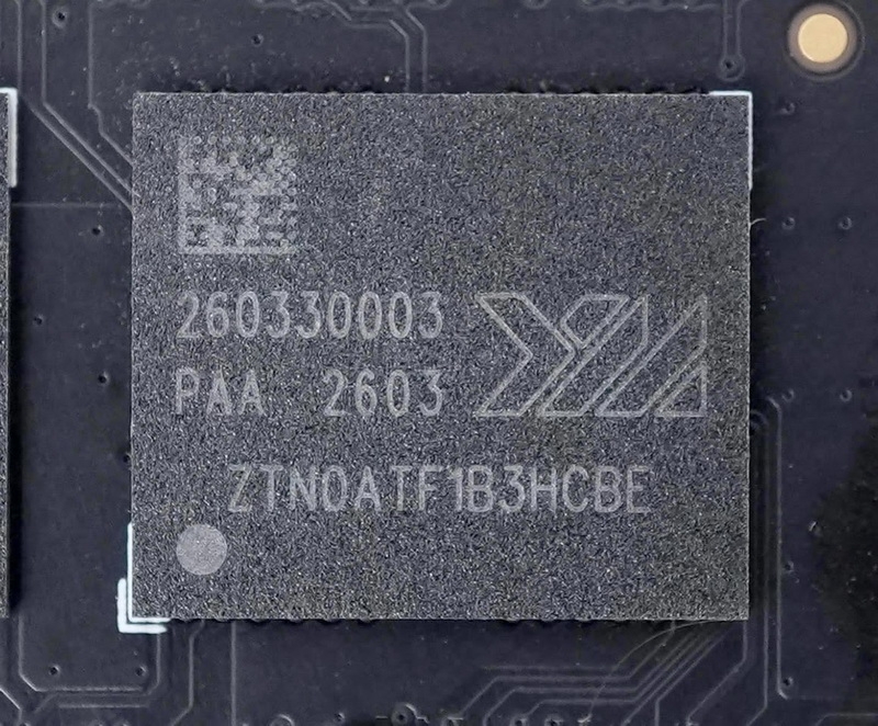
YMTC, a manufacturer primarily known for flash memory, is expanding into the DRAM market. The company has already begun small-scale production of LPDDR5X memory, currently outputting approximately 5,000 silicon wafers per month at its Fab 2 facility.
The current production at Fab 2 involves 16 Gbit (2 GB) LPDDR5X chips with data transfer speeds of 7,500 MT/s. YMTC is now preparing to launch full-scale production of LPDDR5X memory featuring 9,600 MT/s speeds at its Fab 3 facility.
The new production process utilizes Vertical Channel Transistor (VCT) technology and a 4F2 layout. YMTC leverages its Xtacking 4.0 technology, which enables the separation of memory cell wafers and peripheral logic wafers, followed by wafer-to-wafer hybrid bonding.
While Micron has stated it will maintain a 6F2 architecture until the arrival of 3D DRAM, YMTC and CXMT are prioritizing the 4F2 architecture. This strategic focus may provide Chinese manufacturers with a design advantage despite existing limitations on DUV lithography equipment.