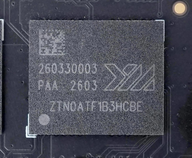

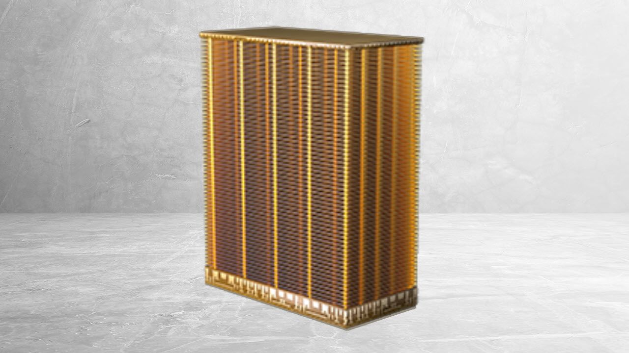
Micron has announced its G11 3D NAND technology, which utilizes wafer-on-wafer bonding to separate the manufacturing of memory arrays and peripheral logic. This approach allows for independent optimization of both components, aiming to improve overall capacity and performance.
The new G11 generation is expected to double the bit density compared to the current G9 (N160) architecture, reaching 42 Gb/mm2. Additionally, the technology will feature an interface speed of 5,400 MT/s, representing a 50% increase over the previous generation.
Micron plans to incorporate more than 400 layers in its G11 memory. The company also expects to reduce energy consumption per bit for data transfers by more than 25%. These advancements are intended for high-capacity SSDs and AI-oriented storage devices.
Mass production of the G11 3D NAND is scheduled to begin in the second half of next year. Further technical specifications are expected to be disclosed by the company in 2027.