SK Hynix is shifting its DRAM production to the 1c nanometer process. In the first quarter of 2026, 1c DRAM will account for approximately 10% of total production. This share is expected to rise to 13% in the second quarter and 24% in the third quarter.
By the fourth quarter of 2026, the 1c process will represent about 34% of output, with a further increase to 35% in the first quarter of 2027. At this point, it will surpass the current main 1b process, which will hold a 33% share, becoming the company's primary production platform.
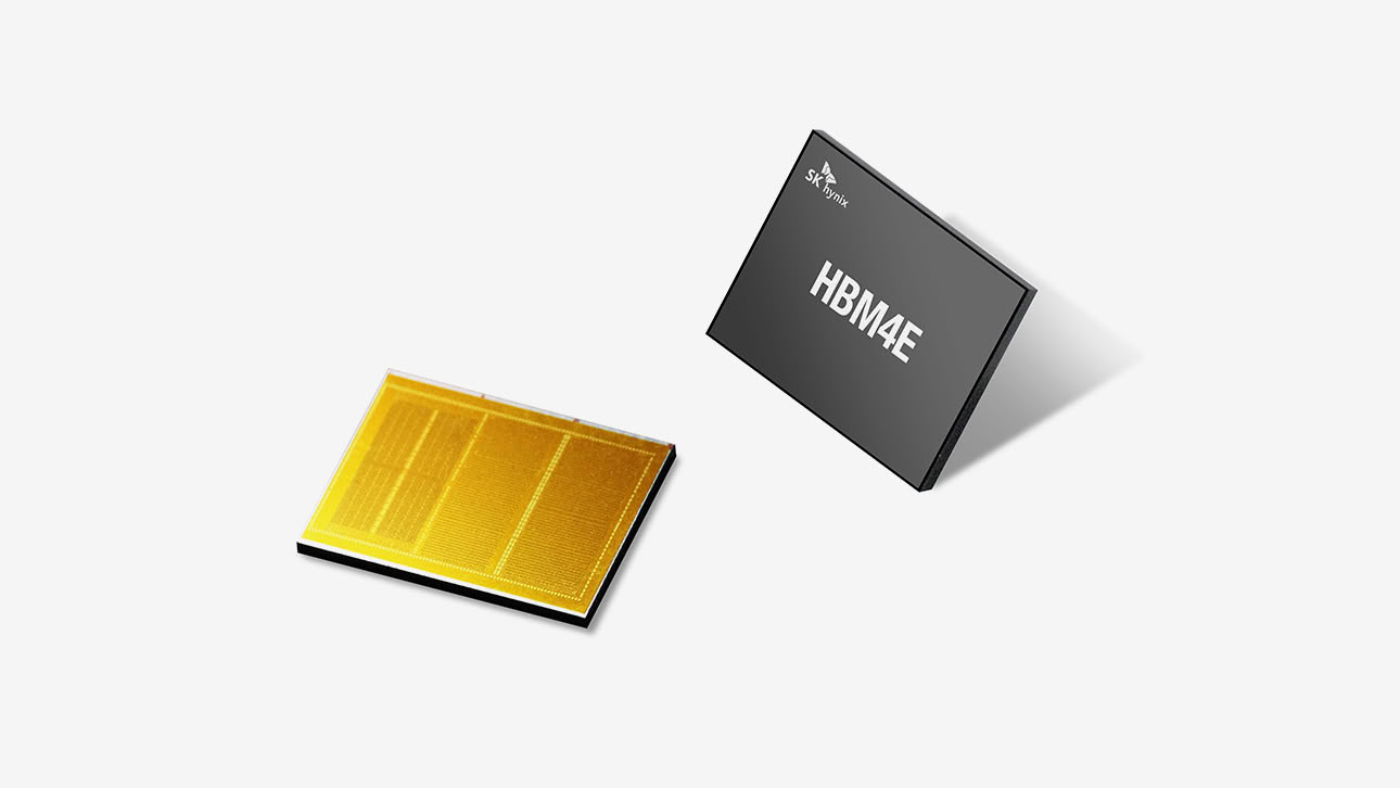
The 1c process features a design size of approximately 11 to 12 nanometers and utilizes 5 to 6 EUV lithography layers. In contrast, the 1b process has a design size of 12 to 1лаnanometers and uses 4 EUV layers. The 1c process will be used to produce HBM4E, LPDDR6, and DDR5 server and desktop memory.
Currently, Samsung Electronics and Micron are ahead in 1c production. Samsung's 1c DRAM output is about 16%, and Micron's is about 19%. SK Hynix expects to overtake them by the fourth quarter of 2026 as it rapidly switches its capacity.
The company is also researching next-generation 4F² vertical gate transistor architectures and 3D DRAM stacking technology to overcome physical limits of the traditional 6F² planar storage cell structure.