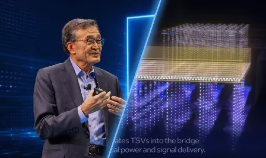
Analyst Jeff Pu from GF Securities suggests that Nvidia may adopt Intel's Foveros packaging technology by the second half of 2028. This forecast aligns with earlier reports from January regarding the upcoming Feynman GPU series, which might utilize Intel's 18A or 14A processes for auxiliary components.
Under this potential arrangement, Intel would handle non-core IP modules or backend assembly processes. The mass production of the 14A process is scheduled for the second half of 2028, matching the analyst's timeline. The core GPU dies would continue to be manufactured by TSMC using advanced lithography nodes.
Intel's Foveros technology enables the vertical stacking of compute dies on a base die, which reduces footprint and improves interconnect efficiency. While Intel continues to compete with TSMC in front-end wafer fabrication, its packaging solutions like EMIB and Foveros are already considered mature in the industry.
Diversifying backend packaging suppliers could help Nvidia mitigate its heavy reliance on TSMC, which currently faces tight capacity constraints due to high global demand for AI accelerators. For Intel, securing such a project would serve as a critical industrial validation for its Foveros packaging architecture.