
Intel executives stated that the company has narrowed the gap in advanced process technology with TSMC to just a few percentage points. CTO Pushkar Ranade noted that the primary challenge is no longer technical performance, but rather scaling manufacturing capacity to match industry leaders.
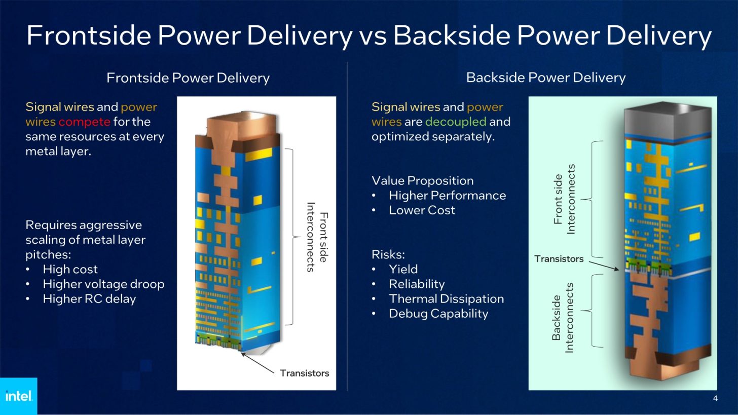
The company is betting on High-NA EUV lithography as a key strategic advantage. Chris Ors, Vice President of Manufacturing and Customer Collaboration, explained that Intel's implementation of backside power delivery allows for more efficient use of High-NA EUV equipment compared to competitors.
Backside power delivery moves the power network to the back of the wafer, freeing up space for transistors and data lines. This architecture reduces complexity and allows Intel to utilize High-NA EUV for patterning, whereas TSMC may still require double-patterning EUV processes due to different architectural constraints.
Intel has officially opened its 14A process node as an option within its Process Design Kit (PDK) for customers. The company plans to engage in individual discussions with clients to determine the adoption of this new technology platform.
While Intel claims its technical capabilities are now comparable to TSMC, the company acknowledges that achieving large-scale, cost-effective production remains a significant long-term hurdle. Intel continues to focus on integrating its power delivery and lithography strategies to regain market competitiveness.