

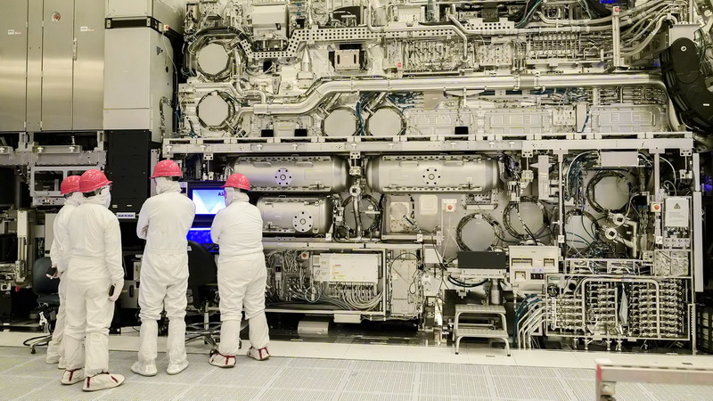
Intel has processed one million 300mm silicon wafers using High-NA EUV lithography. The company is currently the only semiconductor manufacturer actively producing chips with this technology. To achieve this, Intel used ASML TWINSCAN EXE:5000 systems for research and testing of the 14A process, later expanding its use to the 18A node.
For certain Panther Lake processor models, Intel utilizes multiple silicon layers exposed with High-NA instead of relying solely on Low-NA. The company also offers this High-NA configuration to external clients. In collaboration with ASML, Intel Foundry has completed acceptance tests for the 14A process using the TWINSCAN EXE:5200B scanner, the second version of the High-NA EUV scanner.
The company previously reported processing more than 30,000 wafers per quarter. The production cycle has been accelerated by reducing the number of steps required to process a single layer from 40 to fewer than 10. This efficiency gain is critical as High-NA EUV systems from ASML cost approximately $400 million each, while Low-NA equipment is twice as cheap.
While Intel leads in High-NA adoption, competitors are taking a different approach. TSMC maintains that it can remain competitive using existing Low-NA EUV lithography by refining the process across generations. Meanwhile, Samsung Foundry is reportedly postponing the implementation of High-NA EUV for its 1nm process until 2030.