
Intel CTO Pushkar Ranade stated that the company's process technology gap with TSMC has narrowed to within a few percentage points. However, he emphasized that catching up in manufacturing scale remains a slow process, as TSMC currently maintains a significantly larger wafer production capacity than Intel.
Ranade noted that scaling advanced chip production faces global supply chain constraints. He indicated that increasing production tenfold is currently unfeasible due to equipment shortages, particularly for EUV lithography tools, making a twofold increase a more realistic target.
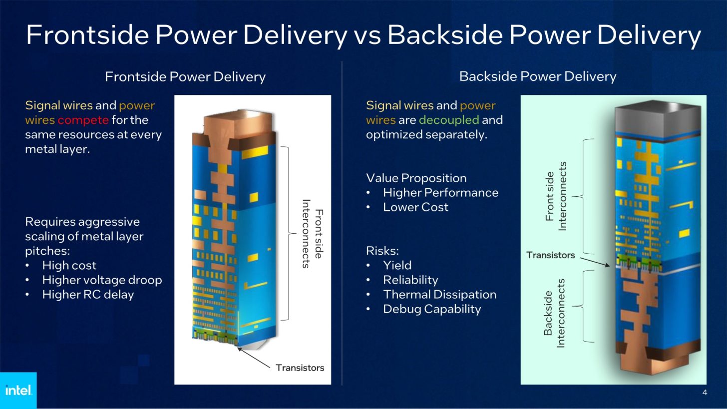
Chris Ors, Vice President of Manufacturing Development at Intel, explained that the company's backside power delivery architecture allows for the integration of High-NA EUV technology. This approach reduces wiring pressure on the front side of the wafer, enabling single-exposure manufacturing for certain layers.
Intel has made High-NA EUV an optional tool in its 14A process design kit for customers. The company plans to evaluate the use of this technology on a case-by-case basis. Additionally, Intel expects to reuse approximately 80% of existing equipment when transitioning from the 18A to the 14A process.